- 您现在的位置:买卖IC网 > PDF目录10133 > LTC2364IMS-18#PBF (Linear Technology)IC ADC 18BIT 250K 1CH 16MSOP PDF资料下载
参数资料
| 型号: | LTC2364IMS-18#PBF |
| 厂商: | Linear Technology |
| 文件页数: | 6/24页 |
| 文件大小: | 0K |
| 描述: | IC ADC 18BIT 250K 1CH 16MSOP |
| 产品培训模块: | LTC2369- 18-/16-bit Pseudo-Differential SAR ADC Family Overview |
| 标准包装: | 37 |
| 位数: | 18 |
| 采样率(每秒): | 250k |
| 数据接口: | 串行,SPI? |
| 转换器数目: | 1 |
| 功率耗散(最大): | 4.25mW |
| 电压电源: | 模拟和数字 |
| 工作温度: | -40°C ~ 85°C |
| 安装类型: | 表面贴装 |
| 封装/外壳: | 16-TFSOP(0.118",3.00mm 宽) |
| 供应商设备封装: | 16-MSOP |
| 包装: | 管件 |
| 输入数目和类型: | 1 个伪差分,单极 |
| 配用: | DC1813A-H-ND - BOARD SAR ADC LTC2364-18 |
LTC2364-18
14
236418f
APPLICATIONS INFORMATION
Power Supply Sequencing
The LTC2364-18 does not have any specific power supply
sequencing requirements. Care should be taken to adhere
to the maximum voltage relationships described in the
Absolute Maximum Ratings section. The LTC2364-18
has a power-on-reset (POR) circuit that will reset the
LTC2364-18 at initial power-up or whenever the power
supply voltage drops below 1V. Once the supply voltage
re-enters the nominal supply voltage range, the POR will
reinitialize the ADC. No conversions should be initiated
until 20s after a POR event to ensure the reinitialization
period has ended. Any conversions initiated before this
time will produce invalid results.
TIMING AND CONTROL
CNV Timing
The LTC2364-18 conversion is controlled by CNV. A ris-
ing edge on CNV will start a conversion and power up the
LTC2364-18.Onceaconversionhasbeeninitiated,itcannot
berestarteduntiltheconversioniscomplete.Foroptimum
performance, CNV should be driven by a clean low jitter
signal. Converter status is indicated by the BUSY output
which remains high while the conversion is in progress.
To ensure that no errors occur in the digitized results, any
additional transitions on CNV should occur within 40ns
from the start of the conversion or after the conversion
has been completed. Once the conversion has completed,
the LTC2364-18 powers down and begins acquiring the
input signal.
Acquisition
AproprietarysamplingarchitectureallowstheLTC2364-18
to begin acquiring the input signal for the next conver-
sion 527ns after the start of the current conversion. This
extends the acquisition time to 3.460s, easing settling
requirements and allowing the use of extremely low power
ADC drivers. (Refer to the Timing Diagram.)
Internal Conversion Clock
The LTC2364-18 has an internal clock that is trimmed to
achieve a maximum conversion time of 3s.
Auto Power-Down
The LTC2364-18 automatically powers down after a
conversion has been completed and powers up once a
new conversion is initiated on the rising edge of CNV.
During power down, data from the last conversion can
be clocked out. To minimize power dissipation during
power down, disable SDO and turn off SCK. The auto
power-down feature will reduce the power dissipation of
the LTC2364-18 as the sampling frequency is reduced.
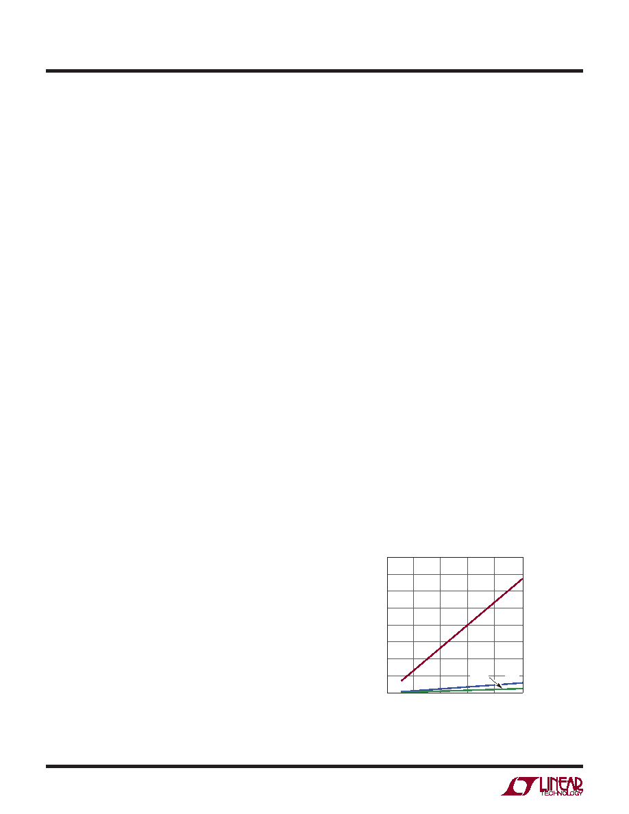
Since power is consumed only during a conversion, the
LTC2364-18remainspowereddownforalargerfractionof
the conversion cycle (tCYC) at lower sample rates, thereby
reducing the average power dissipation which scales with
the sampling rate as shown in Figure 9.
DIGITAL INTERFACE
The LTC2364-18 has a serial digital interface. The flexible
OVDD supply allows the LTC2364-18 to communicate with
any digital logic operating between 1.8V and 5V, including
2.5V and 3.3V systems.
The serial output data is clocked out on the SDO pin when
anexternalclockisappliedtotheSCKpinifSDOisenabled.
Clocking out the data after the conversion will yield the
best performance. With a shift clock frequency of at least
20MHz, a 250ksps throughput is still achieved. The serial
output data changes state on the rising edge of SCK and
can be captured on the falling edge or next rising edge of
SCK. D17 remains valid till the first rising edge of SCK.
Figure 9. Power Supply Current of the LTC2364-18
Versus Sampling Rate
SAMPLING RATE (kHz)
1
0
POWER
SUPPLY
CURRENT
(mA)
0.2
0.4
0.6
0.8
1.2
1.6
1.0
1.4
50
100
150
200
IVDD
236418 F09
250
IOVDD
IREF
相关PDF资料 |
PDF描述 |
|---|---|
| LT1791IN | IC TXRX RS485/RS422 60V 14-DIP |
| IDT72401L15SO | IC FIFO PAR 64X4 15NS 16-SOIC |
| LT1328CS8 | IC RECEIVER 4MBPS IRDA IR 8-SOIC |
| IDT7203L25JI8 | IC MEM FIFO 2048X9 25NS 32-PLCC |
| ADM237LANZ | IC TXRX RS-232 5:3 5V LP 24DIP |
相关代理商/技术参数 |
参数描述 |
|---|---|
| LTC2365CS6#PBF | 制造商:Linear Technology 功能描述:MS-ADC/General Purpose, Cut Tape 12-bit 1Msps SAR ADC in TSOT-6 |
| LTC2365CS6#TRMPBF | 功能描述:IC ADC 12BIT 1MSPS TSOT23-6 RoHS:是 类别:集成电路 (IC) >> 数据采集 - 模数转换器 系列:- 标准包装:1 系列:microPOWER™ 位数:8 采样率(每秒):1M 数据接口:串行,SPI? 转换器数目:1 功率耗散(最大):- 电压电源:模拟和数字 工作温度:-40°C ~ 125°C 安装类型:表面贴装 封装/外壳:24-VFQFN 裸露焊盘 供应商设备封装:24-VQFN 裸露焊盘(4x4) 包装:Digi-Reel® 输入数目和类型:8 个单端,单极 产品目录页面:892 (CN2011-ZH PDF) 其它名称:296-25851-6 |
| LTC2365CS6#TRPBF | 功能描述:IC ADC 12BIT 1MSPS TSOT23-6 RoHS:是 类别:集成电路 (IC) >> 数据采集 - 模数转换器 系列:- 标准包装:2,500 系列:- 位数:16 采样率(每秒):15 数据接口:MICROWIRE?,串行,SPI? 转换器数目:1 功率耗散(最大):480µW 电压电源:单电源 工作温度:-40°C ~ 85°C 安装类型:表面贴装 封装/外壳:38-WFQFN 裸露焊盘 供应商设备封装:38-QFN(5x7) 包装:带卷 (TR) 输入数目和类型:16 个单端,双极;8 个差分,双极 配用:DC1011A-C-ND - BOARD DELTA SIGMA ADC LTC2494 |
| LTC2365CTS8#TRMPBF | 功能描述:IC ADC 12BIT 1MSPS TSOT23-8 RoHS:是 类别:集成电路 (IC) >> 数据采集 - 模数转换器 系列:- 产品培训模块:Data Converter Basics 标准包装:1,000 系列:- 位数:10 采样率(每秒):30M 数据接口:并联 转换器数目:1 功率耗散(最大):150mW 电压电源:模拟和数字 工作温度:0°C ~ 70°C 安装类型:表面贴装 封装/外壳:28-SOIC(0.295",7.50mm 宽) 供应商设备封装:28-SOIC 包装:带卷 (TR) 输入数目和类型:1 个单端,单极 配用:296-10003-ND - EVAL MOD FOR THS1030296-10004-ND - EVAL MOD FOR THS1031 |
| LTC2365CTS8#TRPBF | 功能描述:IC ADC 12BIT 1MSPS TSOT23-8 RoHS:是 类别:集成电路 (IC) >> 数据采集 - 模数转换器 系列:- 标准包装:2,500 系列:- 位数:16 采样率(每秒):15 数据接口:MICROWIRE?,串行,SPI? 转换器数目:1 功率耗散(最大):480µW 电压电源:单电源 工作温度:-40°C ~ 85°C 安装类型:表面贴装 封装/外壳:38-WFQFN 裸露焊盘 供应商设备封装:38-QFN(5x7) 包装:带卷 (TR) 输入数目和类型:16 个单端,双极;8 个差分,双极 配用:DC1011A-C-ND - BOARD DELTA SIGMA ADC LTC2494 |
发布紧急采购,3分钟左右您将得到回复。