- 您现在的位置:买卖IC网 > PDF目录10298 > LTC2411-1CMS#TRPBF (Linear Technology)IC A/DCONV DIFF INPUT&REF 10MSOP PDF资料下载
参数资料
| 型号: | LTC2411-1CMS#TRPBF |
| 厂商: | Linear Technology |
| 文件页数: | 15/40页 |
| 文件大小: | 0K |
| 描述: | IC A/DCONV DIFF INPUT&REF 10MSOP |
| 标准包装: | 2,500 |
| 位数: | 24 |
| 采样率(每秒): | 6.8 |
| 数据接口: | MICROWIRE?,串行,SPI? |
| 转换器数目: | 2 |
| 功率耗散(最大): | 1mW |
| 电压电源: | 单电源 |
| 工作温度: | 0°C ~ 70°C |
| 安装类型: | 表面贴装 |
| 封装/外壳: | 10-TFSOP,10-MSOP(0.118",3.00mm 宽) |
| 供应商设备封装: | 10-MSOP |
| 包装: | 带卷 (TR) |
| 输入数目和类型: | 1 个差分,双极 |
第1页第2页第3页第4页第5页第6页第7页第8页第9页第10页第11页第12页第13页第14页当前第15页第16页第17页第18页第19页第20页第21页第22页第23页第24页第25页第26页第27页第28页第29页第30页第31页第32页第33页第34页第35页第36页第37页第38页第39页第40页
LTC2411/LTC2411-1
22
Particular attention must be given to the connection of the
FO signal when the LTC2411/LTC2411-1 are used with an
external conversion clock. This clock is active during the
conversion time and the normal mode rejection provided
by the internal digital filter is not very high at this fre-
quency. A normal mode signal of this frequency at the
converter reference terminals may result into DC gain and
INL errors. A normal mode signal of this frequency at the
converter input terminals may result into a DC offset error.
Such perturbations may occur due to asymmetric capaci-
tive coupling between the FO signal trace and the converter
input and/or reference connection traces. An immediate
solution is to maintain maximum possible separation
between the FO signal trace and the input/reference sig-
nals. When the FO signal is parallel terminated near the
converter, substantial AC current is flowing in the loop
formed by the FO connection trace, the termination and the
ground return path. Thus, perturbation signals may be
inductively coupled into the converter input and/or refer-
ence. In this situation, the user must reduce to a minimum
the loop area for the FO signal as well as the loop area for
the differential input and reference connections.
Driving the Input and Reference
The input and reference pins of the LTC2411/LTC2411-1
converter are directly connected to a network of sampling
capacitors. Depending upon the relation between the dif-
ferential input voltage and the differential reference volt-
age, these capacitors are switching between these four
pins transfering small amounts of charge in the process.
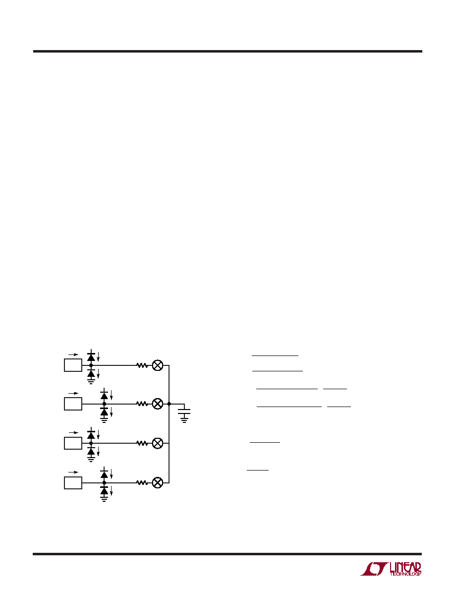
A simplified equivalent circuit is shown in Figure 11.
For a simple approximation, the source impedance RS
driving an analog input pin (IN+, IN–, REF+ or REF–) can be
considered to form, together with RSW and CEQ (see
Figure 11), a first order passive network with a time
constant
τ = (RS + RSW) CEQ. The converter is able to
sample the input signal with better than 1ppm accuracy if
the sampling period is at least 14 times greater than the
input circuit time constant
τ. The sampling process on the
four input analog pins is quasi-independent so each time
constant should be considered by itself and, under worst-
case circumstances, the errors may add.
When using the internal oscillator (FO = LOW or HIGH), the
LTC2411 (LTC2411-1)’s front-end switched-capacitor net-
work is clocked at 76800Hz (69900Hz) corresponding to
APPLICATIO S I FOR ATIO
WU
UU
Figure 11. LTC2411/LTC2411-1 Equivalent Analog Input Circuit
VREF+
VIN+
VCC
RSW (TYP)
20k
ILEAK
VCC
ILEAK
VCC
RSW (TYP)
20k
CEQ
6pF
(TYP)
RSW (TYP)
20k
ILEAK
IIN+
VIN–
IIN–
IREF+
IREF–
2411 F11
ILEAK
VCC
ILEAK
SWITCHING FREQUENCY
fSW = 76800Hz INTERNAL OSCILLATOR (FO = LOW OR HIGH)
fSW = 0.5 fEOSC EXTERNAL OSCILLATOR
VREF–
RSW (TYP)
20k
IIN
VV
V
R
IIN
VV
V
R
I REF
VV
V
R
V
VR
I REF
VV
V
R
V
VR
where
AVG
IN
INCM
REFCM
EQ
AVG
IN
INCM
REFCM
EQ
AVG
REF
INCM
REFCM
EQ
IN
REF
EQ
AVG
REF
INCM
REFCM
EQ
IN
REF
EQ
+
+
() = +
() = +
() =
+
() =
+
+
05
15
05
15
05
2
.
::
.
V
REF
V
REF
VIN
IN
V
IN
R
M
INTERNAL OSCILLATOR
Hz Notch F
LOW LTC
R
M
INTERNAL OSCILLATOR
Hz Notch F
HIGH LTC
R
M
INTERNAL OSCILLATOR F
LOW LTC
REF
REFCM
IN
INCM
EQ
O
EQ
O
EQ
O
=
+
=
==
()(
)
==
()(
)
==
()
+
2
10 8
60
2411
13 0
50
2411
11 9
2411
2411 1
167 1012
()
=
()
R
f
EXTERNAL OSCILLATOR
EQ
EOSC
./
相关PDF资料 |
PDF描述 |
|---|---|
| D38999/26JB98SBLC | CONN HSG PLUG 6POS STRGHT SCKT |
| VE-B3H-MY | CONVERTER MOD DC/DC 52V 50W |
| MS27484E18F53SLC | CONN HSG PLUG 53POS STRGHT SCKT |
| LTC2415-1CGN#TRPBF | IC ADC 24BIT DIFFINPUT/REF16SSOP |
| LTC2415CGN#TRPBF | IC A/D CONV 24BIT MICRPWR 16SSOP |
相关代理商/技术参数 |
参数描述 |
|---|---|
| LTC2411-1IMS | 功能描述:IC A/DCONV DIFF INPUT&REF 10MSOP RoHS:否 类别:集成电路 (IC) >> 数据采集 - 模数转换器 系列:- 标准包装:1,000 系列:- 位数:16 采样率(每秒):45k 数据接口:串行 转换器数目:2 功率耗散(最大):315mW 电压电源:模拟和数字 工作温度:0°C ~ 70°C 安装类型:表面贴装 封装/外壳:28-SOIC(0.295",7.50mm 宽) 供应商设备封装:28-SOIC W 包装:带卷 (TR) 输入数目和类型:2 个单端,单极 |
| LTC2411-1IMS#PBF | 功能描述:IC A/DCONV DIFF INPUT&REF 10MSOP RoHS:是 类别:集成电路 (IC) >> 数据采集 - 模数转换器 系列:- 标准包装:1,000 系列:- 位数:16 采样率(每秒):45k 数据接口:串行 转换器数目:2 功率耗散(最大):315mW 电压电源:模拟和数字 工作温度:0°C ~ 70°C 安装类型:表面贴装 封装/外壳:28-SOIC(0.295",7.50mm 宽) 供应商设备封装:28-SOIC W 包装:带卷 (TR) 输入数目和类型:2 个单端,单极 |
| LTC2411-1IMS#TR | 功能描述:IC A/DCONV DIFF INPUT&REF 10MSOP RoHS:否 类别:集成电路 (IC) >> 数据采集 - 模数转换器 系列:- 标准包装:1,000 系列:- 位数:16 采样率(每秒):45k 数据接口:串行 转换器数目:2 功率耗散(最大):315mW 电压电源:模拟和数字 工作温度:0°C ~ 70°C 安装类型:表面贴装 封装/外壳:28-SOIC(0.295",7.50mm 宽) 供应商设备封装:28-SOIC W 包装:带卷 (TR) 输入数目和类型:2 个单端,单极 |
| LTC2411-1IMS#TRPBF | 功能描述:IC A/DCONV DIFF INPUT&REF 10MSOP RoHS:是 类别:集成电路 (IC) >> 数据采集 - 模数转换器 系列:- 产品培训模块:Lead (SnPb) Finish for COTS Obsolescence Mitigation Program 标准包装:2,500 系列:- 位数:12 采样率(每秒):3M 数据接口:- 转换器数目:- 功率耗散(最大):- 电压电源:- 工作温度:- 安装类型:表面贴装 封装/外壳:SOT-23-6 供应商设备封装:SOT-23-6 包装:带卷 (TR) 输入数目和类型:- |
| LTC2411CMS | 功能描述:IC A/D CONV 24BIT MICRPWR 10MSOP RoHS:否 类别:集成电路 (IC) >> 数据采集 - 模数转换器 系列:- 标准包装:1,000 系列:- 位数:16 采样率(每秒):45k 数据接口:串行 转换器数目:2 功率耗散(最大):315mW 电压电源:模拟和数字 工作温度:0°C ~ 70°C 安装类型:表面贴装 封装/外壳:28-SOIC(0.295",7.50mm 宽) 供应商设备封装:28-SOIC W 包装:带卷 (TR) 输入数目和类型:2 个单端,单极 |
发布紧急采购,3分钟左右您将得到回复。