- 您现在的位置:买卖IC网 > PDF目录10298 > LTC2411-1CMS#TRPBF (Linear Technology)IC A/DCONV DIFF INPUT&REF 10MSOP PDF资料下载
参数资料
| 型号: | LTC2411-1CMS#TRPBF |
| 厂商: | Linear Technology |
| 文件页数: | 16/40页 |
| 文件大小: | 0K |
| 描述: | IC A/DCONV DIFF INPUT&REF 10MSOP |
| 标准包装: | 2,500 |
| 位数: | 24 |
| 采样率(每秒): | 6.8 |
| 数据接口: | MICROWIRE?,串行,SPI? |
| 转换器数目: | 2 |
| 功率耗散(最大): | 1mW |
| 电压电源: | 单电源 |
| 工作温度: | 0°C ~ 70°C |
| 安装类型: | 表面贴装 |
| 封装/外壳: | 10-TFSOP,10-MSOP(0.118",3.00mm 宽) |
| 供应商设备封装: | 10-MSOP |
| 包装: | 带卷 (TR) |
| 输入数目和类型: | 1 个差分,双极 |
第1页第2页第3页第4页第5页第6页第7页第8页第9页第10页第11页第12页第13页第14页第15页当前第16页第17页第18页第19页第20页第21页第22页第23页第24页第25页第26页第27页第28页第29页第30页第31页第32页第33页第34页第35页第36页第37页第38页第39页第40页
LTC2411/LTC2411-1
23
a 13
s (14.2s) sampling period. Thus, for settling errors
of less than 1ppm, the driving source impedance should
be chosen such that
τ ≤ 13s/14 = 920ns (1.02s). When
an external oscillator of frequency fEOSC is used, the
sampling period is 2/fEOSC and, for a settling error of less
than 1ppm,
τ ≤ 0.14/fEOSC.
Input Current
If complete settling occurs on the input, conversion re-
sults will be unaffected by the dynamic input current. An
incomplete settling of the input signal sampling process
may result in gain and offset errors, but it will not degrade
the INL performance of the converter. Figure 11 shows the
mathematical expressions for the average bias currents
flowing through the IN+ and IN– pins as a result of the
sampling charge transfers when integrated over a sub-
stantial time period (longer than 64 internal clock cycles).
The effect of this input dynamic current can be analyzed
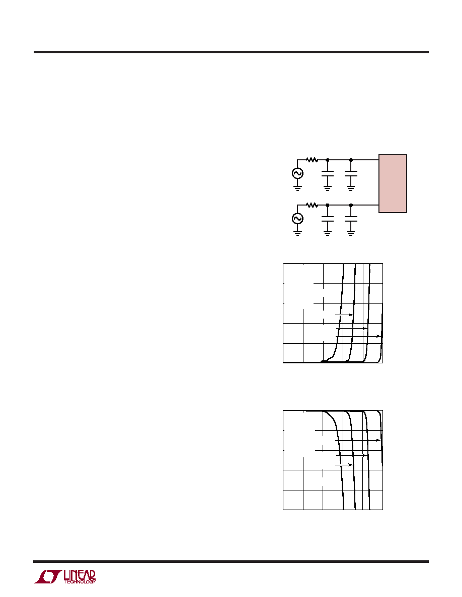
using the test circuit of Figure 12. The CPAR capacitor
includes the LTC2411/LTC2411-1 pin capacitance (5pF
typical) plus the capacitance of the test fixture used to
obtain the results shown in Figures 13 and 14. A careful
implementation can bring the total input capacitance (CIN
+ CPAR) closer to 5pF thus achieving better performance
than the one predicted by Figures 13 and 14. The effect of
the input dynamic current is almost the same for the
LTC2411 and the LTC2411-1 and measurements of the
LTC2411 with FO = GND are plotted out as a typical case.
For simplicity, two distinct situations can be considered.
For relatively small values of input capacitance (CIN <
0.01
F), the voltage on the sampling capacitor settles
almost completely and relatively large values for the
source impedance result in only small errors. Such values
for CIN will deteriorate the converter offset and gain
performance without significant benefits of signal filter-
ing and the user is advised to avoid them. Nevertheless,
when small values of CIN are unavoidably present as
parasitics of input multiplexers, wires, connectors or
sensors, the LTC2411/LTC2411-1 can maintain their ex-
ceptional accuracy while operating with relative large
values of source resistance as shown in Figures 13 and
14. These measured results may be slightly different from
the first order approximation suggested earlier because
they include the effect of the actual second order input
network together with the nonlinear settling process of
the input amplifiers. For small CIN values, the settling on
IN+ and IN– occurs almost independently and there is little
benefit in trying to match the source impedance for the
two pins.
APPLICATIO S I FOR ATIO
WU
UU
CIN
2411 F12
VINCM + 0.5VIN
RSOURCE
CPAR
20pF
CIN
VINCM – 0.5VIN
RSOURCE
CPAR
20pF
IN+
IN –
LTC2411/
LTC2411-1
RSOURCE ()
1
10
100
1k
10k
100k
+FS
ERROR
(ppm
OF
V
REF
)
2411 F13
50
40
30
20
10
0
VCC = 5V
REF+ = 5V
REF– = GND
IN+ = 5V
IN– = 2.5V
FO = GND
TA = 25°C
CIN = 0.01F
CIN = 0pF
CIN = 0.001F
CIN = 100pF
RSOURCE ()
1
10
100
1k
10k
100k
–
FS
ERROR
(ppm
OF
V
REF
)
2411 F14
0
–10
–20
–30
–40
–50
VCC = 5V
REF+ = 5V
REF – = GND
IN+ = GND
IN– = 2.5V
FO = GND
TA = 25°C
CIN = 0pF
CIN = 0.001F
CIN = 100pF
CIN = 0.01F
Figure 12. An RC Network at IN+ and IN–
Figure 13. +FS Error vs RSOURCE at IN+ or IN– (Small CIN)
Figure 14. –FS Error vs RSOURCE at IN
+ or IN– (Small CIN)
相关PDF资料 |
PDF描述 |
|---|---|
| D38999/26JB98SBLC | CONN HSG PLUG 6POS STRGHT SCKT |
| VE-B3H-MY | CONVERTER MOD DC/DC 52V 50W |
| MS27484E18F53SLC | CONN HSG PLUG 53POS STRGHT SCKT |
| LTC2415-1CGN#TRPBF | IC ADC 24BIT DIFFINPUT/REF16SSOP |
| LTC2415CGN#TRPBF | IC A/D CONV 24BIT MICRPWR 16SSOP |
相关代理商/技术参数 |
参数描述 |
|---|---|
| LTC2411-1IMS | 功能描述:IC A/DCONV DIFF INPUT&REF 10MSOP RoHS:否 类别:集成电路 (IC) >> 数据采集 - 模数转换器 系列:- 标准包装:1,000 系列:- 位数:16 采样率(每秒):45k 数据接口:串行 转换器数目:2 功率耗散(最大):315mW 电压电源:模拟和数字 工作温度:0°C ~ 70°C 安装类型:表面贴装 封装/外壳:28-SOIC(0.295",7.50mm 宽) 供应商设备封装:28-SOIC W 包装:带卷 (TR) 输入数目和类型:2 个单端,单极 |
| LTC2411-1IMS#PBF | 功能描述:IC A/DCONV DIFF INPUT&REF 10MSOP RoHS:是 类别:集成电路 (IC) >> 数据采集 - 模数转换器 系列:- 标准包装:1,000 系列:- 位数:16 采样率(每秒):45k 数据接口:串行 转换器数目:2 功率耗散(最大):315mW 电压电源:模拟和数字 工作温度:0°C ~ 70°C 安装类型:表面贴装 封装/外壳:28-SOIC(0.295",7.50mm 宽) 供应商设备封装:28-SOIC W 包装:带卷 (TR) 输入数目和类型:2 个单端,单极 |
| LTC2411-1IMS#TR | 功能描述:IC A/DCONV DIFF INPUT&REF 10MSOP RoHS:否 类别:集成电路 (IC) >> 数据采集 - 模数转换器 系列:- 标准包装:1,000 系列:- 位数:16 采样率(每秒):45k 数据接口:串行 转换器数目:2 功率耗散(最大):315mW 电压电源:模拟和数字 工作温度:0°C ~ 70°C 安装类型:表面贴装 封装/外壳:28-SOIC(0.295",7.50mm 宽) 供应商设备封装:28-SOIC W 包装:带卷 (TR) 输入数目和类型:2 个单端,单极 |
| LTC2411-1IMS#TRPBF | 功能描述:IC A/DCONV DIFF INPUT&REF 10MSOP RoHS:是 类别:集成电路 (IC) >> 数据采集 - 模数转换器 系列:- 产品培训模块:Lead (SnPb) Finish for COTS Obsolescence Mitigation Program 标准包装:2,500 系列:- 位数:12 采样率(每秒):3M 数据接口:- 转换器数目:- 功率耗散(最大):- 电压电源:- 工作温度:- 安装类型:表面贴装 封装/外壳:SOT-23-6 供应商设备封装:SOT-23-6 包装:带卷 (TR) 输入数目和类型:- |
| LTC2411CMS | 功能描述:IC A/D CONV 24BIT MICRPWR 10MSOP RoHS:否 类别:集成电路 (IC) >> 数据采集 - 模数转换器 系列:- 标准包装:1,000 系列:- 位数:16 采样率(每秒):45k 数据接口:串行 转换器数目:2 功率耗散(最大):315mW 电压电源:模拟和数字 工作温度:0°C ~ 70°C 安装类型:表面贴装 封装/外壳:28-SOIC(0.295",7.50mm 宽) 供应商设备封装:28-SOIC W 包装:带卷 (TR) 输入数目和类型:2 个单端,单极 |
发布紧急采购,3分钟左右您将得到回复。