- 您现在的位置:买卖IC网 > PDF目录2006 > LTC2418IGN#TRPBF (Linear Technology)IC ADC 24BIT DIFF INPUT 28SSOP PDF资料下载
参数资料
| 型号: | LTC2418IGN#TRPBF |
| 厂商: | Linear Technology |
| 文件页数: | 15/48页 |
| 文件大小: | 0K |
| 描述: | IC ADC 24BIT DIFF INPUT 28SSOP |
| 标准包装: | 2,500 |
| 位数: | 24 |
| 采样率(每秒): | 7.5 |
| 数据接口: | MICROWIRE?,串行,SPI? |
| 转换器数目: | 1 |
| 功率耗散(最大): | 1mW |
| 电压电源: | 单电源 |
| 工作温度: | -40°C ~ 85°C |
| 安装类型: | 表面贴装 |
| 封装/外壳: | 28-SSOP(0.154",3.90mm 宽) |
| 供应商设备封装: | 28-SSOP |
| 包装: | 带卷 (TR) |
| 输入数目和类型: | 16 个单端,单极;16 个单端,双极;8 个差分,单极;8 个差分,双极 |
| 配用: | DC571A-ND - BOARD DELTA SIGMA ADC LTC2418 |
第1页第2页第3页第4页第5页第6页第7页第8页第9页第10页第11页第12页第13页第14页当前第15页第16页第17页第18页第19页第20页第21页第22页第23页第24页第25页第26页第27页第28页第29页第30页第31页第32页第33页第34页第35页第36页第37页第38页第39页第40页第41页第42页第43页第44页第45页第46页第47页第48页
LTC2414/LTC2418
22
241418fa
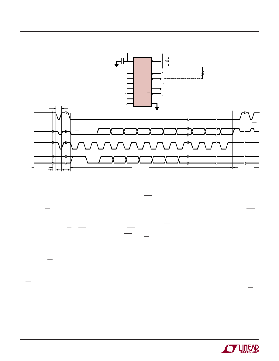
When testing EOC, if the conversion is complete (EOC = 0),
the device will exit the low power mode during the EOC
test. In order to allow the device to return to the low power
sleep state, CS must be pulled HIGH before the first rising
edge of SCK. In the internal SCK timing mode, SCK goes
HIGH and the device begins outputting data at time tEOCtest
after the falling edge of CS (if EOC = 0) or tEOCtest after EOC
goes LOW (if CS is LOW during the falling edge of EOC).
The value of tEOCtest is 23s if the device is using its internal
oscillator (FO = logic LOW or HIGH). If FO is driven by an
external oscillator of frequency fEOSC, then tEOCtest is
3.6/fEOSC. If CS is pulled HIGH before time tEOCtest, the
device returns to the sleep state and the conversion result
is held in the internal static shift register.
If CS remains LOW longer than tEOCtest, the first rising
edge of SCK will occur and the conversion result is serially
shifted out of the SDO pin. The data I/O cycle concludes
after the 32nd rising edge. The input data is then shifted in
via the SDI pin on the rising edge of SCK (including the first
rising edge) and the output data is shifted out of the SDO
pin on each falling edge of SCK. The internally generated
serial clock is output to the SCK pin. This signal may be
used to shift the conversion result into external circuitry.
EOC can be latched on the first rising edge of SCK and the
last bit of the conversion result on the 32nd rising edge of
SCK. After the 32nd rising edge, SDO goes HIGH (EOC =
1), SCK stays HIGH and a new conversion starts.
Typically, CS remains LOW during the data output state.
However, the data output state may be aborted by pulling
CS HIGH anytime between the first and 32nd rising edge
of SCK, see Figure 9. On the rising edge of CS, the device
aborts the data output state and immediately initiates a
new conversion. If the device has not finished loading the
last input bit A0 of SDI by the time CS is pulled HIGH, the
address information is discarded and the previous ad-
dress is still kept. This is useful for systems not requiring
all 32 bits of output data, aborting an invalid conversion
cycle, or synchronizing the start of a conversion. If CS is
pulled HIGH while the converter is driving SCK LOW, the
internal pull-up is not available to restore SCK to a logic
HIGH state. This will cause the device to exit the internal
serial clock mode on the next falling edge of CS. This can
be avoided by adding an external 10k pull-up resistor to
the SCK pin or by never pulling CS HIGH when SCK is LOW.
APPLICATIO S I FOR ATIO
WU
UU
Figure 8. Internal Serial Clock, Single Cycle Operation
(1)
(0)
EN
SGL
A2
A1
A0
ODD/
SIGN
SDI
DON’T CARE
SDO
SCK
(INTERNAL)
CS
MSB
SIG
BIT 0
LSB
PARITY
BIT 6
TEST EOC
BIT 27
BIT 26
BIT 25
BIT 24
BIT 28
BIT 29
BIT 30
EOC
BIT 31
SLEEP
DATA OUTPUT
CONVERSION
241418 F08
<tEOCtest
Hi-Z
TEST EOC
VCC
FO
REF+
REF–
CH0
CH7
CH8
CH15
COM
SCK
SDI
SDO
CS
GND
919
11
12
21
28
1
8
10
18
17
15
16
20
REFERENCE
VOLTAGE
0.1V TO VCC
ANALOG
INPUTS
= 50Hz REJECTION
= EXTERNAL OSCILLATOR
= 60Hz REJECTION
VCC
1
F
2.7V TO 5.5V
LTC2414/
LTC2418
4-WIRE
SPI INTERFACE
VCC
10k
相关PDF资料 |
PDF描述 |
|---|---|
| LTC2431IMS#TRPBF | IC ADC 20BIT DIFFINPUT/REF10MSOP |
| LTC2433-1IMS#TRPBF | IC ADC DIFF 16BIT 3WIRE 10-MSOP |
| LTC2435CGN#TRPBF | IC ADC DIFF I/REF 20BIT 16-SSOP |
| LTC2442IG#PBF | IC ADC 24BIT 4CH 36-SSOP |
| LTC2446IUHF#TRPBF | IC ADC 24BIT 8CH HI SPEED 38QFN |
相关代理商/技术参数 |
参数描述 |
|---|---|
| LTC2420CS8 | 功能描述:IC ADC 20BIT MICRPWR W/OSC 8SOIC RoHS:否 类别:集成电路 (IC) >> 数据采集 - 模数转换器 系列:- 标准包装:1,000 系列:- 位数:16 采样率(每秒):45k 数据接口:串行 转换器数目:2 功率耗散(最大):315mW 电压电源:模拟和数字 工作温度:0°C ~ 70°C 安装类型:表面贴装 封装/外壳:28-SOIC(0.295",7.50mm 宽) 供应商设备封装:28-SOIC W 包装:带卷 (TR) 输入数目和类型:2 个单端,单极 |
| LTC2420CS8#PBF | 功能描述:IC ADC 20BIT MICRPWR W/OSC 8SOIC RoHS:是 类别:集成电路 (IC) >> 数据采集 - 模数转换器 系列:- 标准包装:1 系列:microPOWER™ 位数:8 采样率(每秒):1M 数据接口:串行,SPI? 转换器数目:1 功率耗散(最大):- 电压电源:模拟和数字 工作温度:-40°C ~ 125°C 安装类型:表面贴装 封装/外壳:24-VFQFN 裸露焊盘 供应商设备封装:24-VQFN 裸露焊盘(4x4) 包装:Digi-Reel® 输入数目和类型:8 个单端,单极 产品目录页面:892 (CN2011-ZH PDF) 其它名称:296-25851-6 |
| LTC2420CS8#PBF | 制造商:Linear Technology 功能描述:A/D Converter (A-D) IC |
| LTC2420CS8#TR | 功能描述:IC A/D CONV 20BIT MICRPWR 8-SOIC RoHS:否 类别:集成电路 (IC) >> 数据采集 - 模数转换器 系列:- 标准包装:1,000 系列:- 位数:16 采样率(每秒):45k 数据接口:串行 转换器数目:2 功率耗散(最大):315mW 电压电源:模拟和数字 工作温度:0°C ~ 70°C 安装类型:表面贴装 封装/外壳:28-SOIC(0.295",7.50mm 宽) 供应商设备封装:28-SOIC W 包装:带卷 (TR) 输入数目和类型:2 个单端,单极 |
| LTC2420CS8#TRPBF | 功能描述:IC ADC 20BIT MICRPWR W/OSC 8SOIC RoHS:否 类别:集成电路 (IC) >> 数据采集 - 模数转换器 系列:- 标准包装:1,000 系列:- 位数:16 采样率(每秒):45k 数据接口:串行 转换器数目:2 功率耗散(最大):315mW 电压电源:模拟和数字 工作温度:0°C ~ 70°C 安装类型:表面贴装 封装/外壳:28-SOIC(0.295",7.50mm 宽) 供应商设备封装:28-SOIC W 包装:带卷 (TR) 输入数目和类型:2 个单端,单极 |
发布紧急采购,3分钟左右您将得到回复。