- 您现在的位置:买卖IC网 > PDF目录10317 > LTC2439-1IGN#TR (Linear Technology)IC ADC 16BIT 16CH MCRPWR 28SSOP PDF资料下载
参数资料
| 型号: | LTC2439-1IGN#TR |
| 厂商: | Linear Technology |
| 文件页数: | 16/28页 |
| 文件大小: | 0K |
| 描述: | IC ADC 16BIT 16CH MCRPWR 28SSOP |
| 标准包装: | 2,500 |
| 位数: | 16 |
| 采样率(每秒): | 6.8 |
| 数据接口: | MICROWIRE?,串行,SPI? |
| 转换器数目: | 1 |
| 功率耗散(最大): | 1mW |
| 电压电源: | 单电源 |
| 工作温度: | -40°C ~ 85°C |
| 安装类型: | 表面贴装 |
| 封装/外壳: | 28-SSOP(0.154",3.90mm 宽) |
| 供应商设备封装: | 28-SSOP |
| 包装: | 带卷 (TR) |
| 输入数目和类型: | 16 个单端,双极;8 个差分,双极 |
| 配用: | DC790A-ND - BOARD DELTA SIGMA ADC LTC2439-1 |
第1页第2页第3页第4页第5页第6页第7页第8页第9页第10页第11页第12页第13页第14页第15页当前第16页第17页第18页第19页第20页第21页第22页第23页第24页第25页第26页第27页第28页
LTC2439-1
23
24391fa
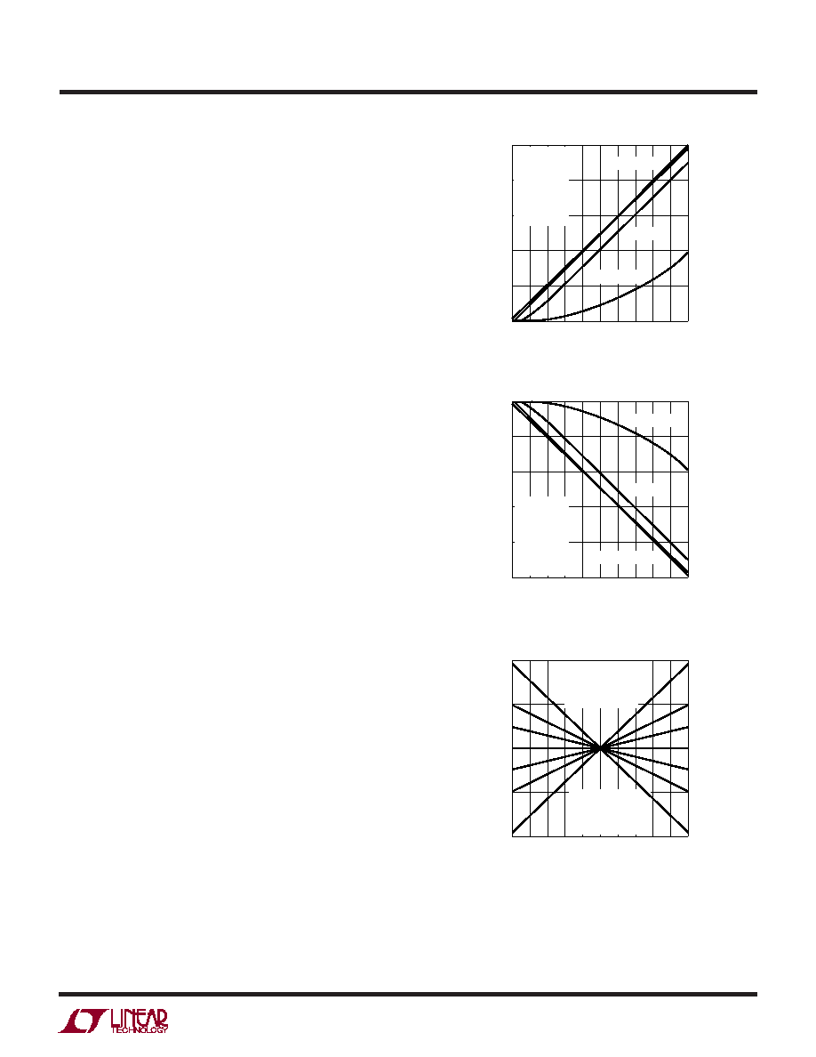
and each ohm of source resistance driving IN+ or IN– will
result in 1.11 10–7 fEOSCLSB gain error at full scale. The
effect of the source resistance on the two input pins is
additive with respect to this gain error. The typical +FS and
–FS errors as a function of the sum of the source resis-
tance seen by IN+ and IN– for large values of CIN are shown
in Figures 16 and 17.
In addition to this gain error, an offset error term may also
appear. The offset error is proportional with the mismatch
between the source impedance driving the two input pins
IN+ and IN– and with the difference between the input and
reference common mode voltages. While the input drive
circuit nonzero source impedance combined with the con-
verter average input current will not degrade the INL
performance, indirect distortion may result from the modu-
lation of the offset error by the common mode component
of the input signal. Thus, when using large CIN capacitor
values, it is advisable to carefully match the source imped-
ance seen by the IN+ and IN– pins. When FO = LOW
(internal oscillator and 50Hz/60Hz notch), every 60
mis-
match in source impedance transforms a full-scale com-
mon mode input signal into a differential mode input
signal of 1LSB. When FO is driven by an external oscillator
with a frequency fEOSC, every 1 mismatch in source
impedance transforms a full-scale common mode input
signal into a differential mode input signal of 1.11 10–7
fEOSCLSB. Figure 18 shows the typical offset error due to
input common mode voltage for various values of source
resistance imbalance between the IN+ and IN– pins when
large CIN values are used.
If possible, it is desirable to operate with the input signal
common mode voltage very close to the reference signal
common mode voltage as is the case in the ratiometric
measurement of a symmetric bridge. This configuration
eliminates the offset error caused by mismatched source
impedances.
The magnitude of the dynamic input current depends upon
the size of the very stable internal sampling capacitors and
upon the accuracy of the converter sampling clock. The
accuracy of the internal clock over the entire temperature
and power supply range is typically better than 0.5%. Such
a specification can also be easily achieved by an external
clock. When relatively stable resistors (50ppm/
°C) are
used for the external source impedance seen by IN+ and
RSOURCE ()
0 100 200 300 400 500 600 700 800 900 1000
+FS
ERROR
(LSB)
24361 F16
20
16
12
8
4
0
VCC = 5V
REF+ = 5V
REF – = GND
IN+ = 3.75V
IN– = 1.25V
FO = GND
TA = 25°C
CIN = 0.01F
CIN = 0.1F
CIN = 1F, 10F
RSOURCE ()
0 100 200 300 400 500 600 700 800 900 1000
–
FS
ERROR
(LSB)
24361 F17
0
–4
–8
–12
–16
–20
VCC = 5V
REF+ = 5V
REF – = GND
IN+ = 1.25V
IN– = 3.75V
FO = GND
TA = 25°C
CIN = 0.01F
CIN = 0.1F
CIN = 1F, 10F
VINCM (V)
0
0.5
1
1.5
2
2.5
3
3.5
4
4.5
5
OFFSET
ERROR
(LSB)
24361 F18
8
4
0
–4
–8
FO = GND
TA = 25°C
RSOURCEIN– = 500
CIN = 10F
VCC = 5V
REF+ = 5V
REF – = GND
IN+ = IN– = VINCM
A:
RIN = +400
B:
RIN = +200
C:
RIN = +100
D:
RIN = 0
E:
RIN = –100
F:
RIN = –200
G:
RIN = –400
A
B
C
D
E
F
G
Figure 16. +FS Error vs RSOURCE at IN+ or IN– (Large CIN)
Figure 17. –FS Error vs RSOURCE at IN+ or IN– (Large CIN)
Figure 18. Offset Error vs Common Mode Voltage
(VINCM = IN+ = IN–) and Input Source Resistance
Imbalance (
RIN = RSOURCEIN+ – RSOURCEIN–) for
Large CIN Values (CIN ≥ 1F)
APPLICATIO S I FOR ATIO
WU
UU
相关PDF资料 |
PDF描述 |
|---|---|
| VE-2T3-MX-S | CONVERTER MOD DC/DC 24V 75W |
| VE-22L-MY | CONVERTER MOD DC/DC 28V 50W |
| MS27467T9F35PD | CONN PLUG 6POS STRAIGHT W/PINS |
| VE-BTK-MW-S | CONVERTER MOD DC/DC 40V 100W |
| VE-22K-MY | CONVERTER MOD DC/DC 40V 50W |
相关代理商/技术参数 |
参数描述 |
|---|---|
| LTC2440CGN | 功能描述:IC ADC DIFFER 24-BIT HS 16-SSOP RoHS:否 类别:集成电路 (IC) >> 数据采集 - 模数转换器 系列:- 标准包装:1,000 系列:- 位数:16 采样率(每秒):45k 数据接口:串行 转换器数目:2 功率耗散(最大):315mW 电压电源:模拟和数字 工作温度:0°C ~ 70°C 安装类型:表面贴装 封装/外壳:28-SOIC(0.295",7.50mm 宽) 供应商设备封装:28-SOIC W 包装:带卷 (TR) 输入数目和类型:2 个单端,单极 |
| LTC2440CGN#PBF | 功能描述:IC ADC DIFFER 24-BIT HS 16-SSOP RoHS:是 类别:集成电路 (IC) >> 数据采集 - 模数转换器 系列:- 标准包装:1 系列:microPOWER™ 位数:8 采样率(每秒):1M 数据接口:串行,SPI? 转换器数目:1 功率耗散(最大):- 电压电源:模拟和数字 工作温度:-40°C ~ 125°C 安装类型:表面贴装 封装/外壳:24-VFQFN 裸露焊盘 供应商设备封装:24-VQFN 裸露焊盘(4x4) 包装:Digi-Reel® 输入数目和类型:8 个单端,单极 产品目录页面:892 (CN2011-ZH PDF) 其它名称:296-25851-6 |
| LTC2440CGN#PBF | 制造商:Linear Technology 功能描述:24BIT ADC DELTA SIG HS 16SSOP 制造商:Linear Technology 功能描述:24BIT ADC, DELTA SIG, HS, 16SSOP |
| LTC2440CGN#TR | 功能描述:IC CONV A/D 24-BIT DIFF 16-SSOP RoHS:否 类别:集成电路 (IC) >> 数据采集 - 模数转换器 系列:- 标准包装:1,000 系列:- 位数:16 采样率(每秒):45k 数据接口:串行 转换器数目:2 功率耗散(最大):315mW 电压电源:模拟和数字 工作温度:0°C ~ 70°C 安装类型:表面贴装 封装/外壳:28-SOIC(0.295",7.50mm 宽) 供应商设备封装:28-SOIC W 包装:带卷 (TR) 输入数目和类型:2 个单端,单极 |
| LTC2440CGN#TRPBF | 功能描述:IC ADC DIFFER 24-BIT HS 16-SSOP RoHS:是 类别:集成电路 (IC) >> 数据采集 - 模数转换器 系列:- 标准包装:1,000 系列:- 位数:16 采样率(每秒):45k 数据接口:串行 转换器数目:2 功率耗散(最大):315mW 电压电源:模拟和数字 工作温度:0°C ~ 70°C 安装类型:表面贴装 封装/外壳:28-SOIC(0.295",7.50mm 宽) 供应商设备封装:28-SOIC W 包装:带卷 (TR) 输入数目和类型:2 个单端,单极 |
发布紧急采购,3分钟左右您将得到回复。