- 您现在的位置:买卖IC网 > PDF目录10252 > LTC2442CG#TRPBF (Linear Technology)IC ADC 24BIT 250MSPS 36-SSOP PDF资料下载
参数资料
| 型号: | LTC2442CG#TRPBF |
| 厂商: | Linear Technology |
| 文件页数: | 3/32页 |
| 文件大小: | 0K |
| 描述: | IC ADC 24BIT 250MSPS 36-SSOP |
| 标准包装: | 2,000 |
| 位数: | 24 |
| 采样率(每秒): | 8k |
| 数据接口: | MICROWIRE?,串行,SPI? |
| 转换器数目: | 1 |
| 功率耗散(最大): | 50mW |
| 电压电源: | 单电源 |
| 工作温度: | 0°C ~ 70°C |
| 安装类型: | 表面贴装 |
| 封装/外壳: | 36-SSOP(0.209",5.30mm 宽) |
| 供应商设备封装: | 36-SSOP |
| 包装: | 带卷 (TR) |
| 输入数目和类型: | 4 个单端,双极;2 个差分,双极 |
| 配用: | DC979A-ND - BOARD DELTA SIGMA ADC LTC2442 |
第1页第2页当前第3页第4页第5页第6页第7页第8页第9页第10页第11页第12页第13页第14页第15页第16页第17页第18页第19页第20页第21页第22页第23页第24页第25页第26页第27页第28页第29页第30页第31页第32页
LTC2442
11
2442fa
For more information www.linear.com/LTC2442
Reference Voltage Range
The LTC2442
DS converter accepts a truly differential
external reference voltage. The absolute/common mode
voltage specification for the REF+ and REF– pins covers
the entire range from GND to VCC. For correct converter
operation, the REF+ pin must always be more positive
than the REF– pin.
The LTC2442 can accept a differential reference voltage
from0.1VtoVCC.Theconverteroutputnoiseisdetermined
by the thermal noise of the front-end circuits, and as such,
its value in microvolts is nearly constant with reference
voltage. A decrease in reference voltage will not signifi-
cantly improve the converter’s effective resolution. On the
other hand, a reduced reference voltage will improve the
converter’s overall INL performance.
Input Voltage Range
The analog input is truly differential with an absolute/
commonmoderangefortheCH0-CH3andCOMinputpins
extending from GND – 0.3V to VCC + 0.3V. Outside these
limits, the ESD protection devices begin to turn on and
the errors due to input leakage current increase rapidly.
Within these limits, the LTC2442 converts the bipolar
differential input signal, VIN = SEL+ – SEL–, from –FS =
–0.5 VREF to +FS = 0.5 VREF where VREF = REF+ – REF–.
Outside this range, the converter indicates the overrange
or the underrange condition using distinct output codes.
Output Data Format
The LTC2442 serial output data stream is 32 bits long.
The first three bits represent status information indicating
the sign and conversion state. The next 24 bits are the
conversion result, MSB first. The remaining five bits are
sub LSBs beyond the 24-bit level that may be included in
averaging or discarded without loss of resolution. In the
case of ultrahigh resolution modes, more than 24 effective
bitsofperformancearepossible(seeTable4).Underthese
conditions, sub LSBs are included in the conversion result
and represent useful information beyond the 24-bit level.
The third and fourth bit together are also used to indicate
an underrange condition (the differential input voltage
is below –FS) or an overrange condition (the differential
input voltage is above +FS).
Bit 31 (first output bit) is the end of conversion (EOC)
indicator. This bit is available at the SDO pin during the
conversion and sleep states whenever the CS pin is LOW.
This bit is HIGH during the conversion and goes LOW
when the conversion is complete.
Bit 30 (second output bit) is a dummy bit (DMY) and is
always LOW.
Bit 29 (third output bit) is the conversion result sign
indicator (SIG). If VIN is >0, this bit is HIGH. If VIN is <0,
this bit is LOW.
Bit28(fourthoutputbit)isthemostsignificantbit(MSB)of
the result. This bit in conjunction with Bit 29 also provides
the underrange or overrange indication. If both Bit 29 and
Bit 28 are HIGH, the differential input voltage is above +FS.
If both Bit 29 and Bit 28 are LOW, the differential input
voltage is below –FS.
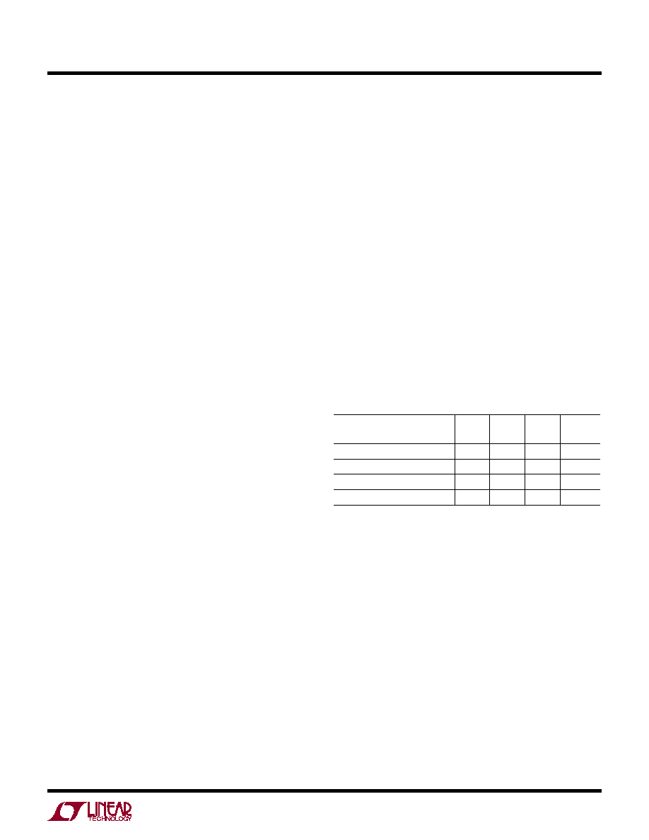
The function of these bits is summarized in Table 1.
Table 1. LTC2442 Status Bits
Input Range
Bit 31
EOC
Bit 30
DMY
Bit 29
SIG
Bit 28
MSB
VIN ≥ 0.5 VREF
0
1
0V ≤ VIN < 0.5 VREF
0
1
0
–0.5 VREF ≤ VIN < 0V
0
1
VIN < –0.5 VREF
0
Bits 28-5 are the 24-bit conversion result MSB first.
Bit 5 is the least significant bit (LSB).
Bits 4-0 are sub LSBs below the 24-bit level. Bits 4-0
may be included in averaging or discarded without loss
of resolution.
Data is shifted out of the SDO pin under control of the
serial clock (SCK), see Figure 3. Whenever CS is HIGH,
SDO remains high impedance and SCK is ignored.
In order to shift the conversion result out of the device,
CS must first be driven LOW. EOC is seen at the SDO pin
of the device once CS is pulled LOW. EOC changes real
time from HIGH to LOW at the completion of a conversion.
This signal may be used as an interrupt for an external
microcontroller. Bit 31 (EOC) can be captured on the first
rising edge of SCK. Bit 30 is shifted out of the device on
applications inForMation
相关PDF资料 |
PDF描述 |
|---|---|
| MS27467E17B35PD | CONN PLUG 55POS STRAIGHT W/PINS |
| IRS20124SPBF | IC DIGITAL AUDIO DRIVER 14-SOIC |
| AD7934BRUZ-REEL7 | IC ADC 12BIT 4CH 1.5MSPS 28TSSOP |
| MS3106F22-23S | CONN PLUG 8POS STRAIGHT W/SCKT |
| MS27467T11F99S | CONN PLUG 7POS STRAIGHT W/SCKT |
相关代理商/技术参数 |
参数描述 |
|---|---|
| LTC2442IG#PBF | 功能描述:IC ADC 24BIT 4CH 36-SSOP RoHS:是 类别:集成电路 (IC) >> 数据采集 - 模数转换器 系列:- 标准包装:1,000 系列:- 位数:12 采样率(每秒):300k 数据接口:并联 转换器数目:1 功率耗散(最大):75mW 电压电源:单电源 工作温度:0°C ~ 70°C 安装类型:表面贴装 封装/外壳:24-SOIC(0.295",7.50mm 宽) 供应商设备封装:24-SOIC 包装:带卷 (TR) 输入数目和类型:1 个单端,单极;1 个单端,双极 |
| LTC2442IG#TRPBF | 功能描述:IC ADC 24BIT 250MSPS 36-SSOP RoHS:是 类别:集成电路 (IC) >> 数据采集 - 模数转换器 系列:- 标准包装:1,000 系列:- 位数:12 采样率(每秒):300k 数据接口:并联 转换器数目:1 功率耗散(最大):75mW 电压电源:单电源 工作温度:0°C ~ 70°C 安装类型:表面贴装 封装/外壳:24-SOIC(0.295",7.50mm 宽) 供应商设备封装:24-SOIC 包装:带卷 (TR) 输入数目和类型:1 个单端,单极;1 个单端,双极 |
| LTC2444CUHF | 功能描述:IC ADC 24BIT HI SPEED 38QFN RoHS:否 类别:集成电路 (IC) >> 数据采集 - 模数转换器 系列:- 标准包装:1,000 系列:- 位数:16 采样率(每秒):45k 数据接口:串行 转换器数目:2 功率耗散(最大):315mW 电压电源:模拟和数字 工作温度:0°C ~ 70°C 安装类型:表面贴装 封装/外壳:28-SOIC(0.295",7.50mm 宽) 供应商设备封装:28-SOIC W 包装:带卷 (TR) 输入数目和类型:2 个单端,单极 |
| LTC2444CUHF#PBF | 功能描述:IC ADC 24BIT HI SPEED 38QFN RoHS:是 类别:集成电路 (IC) >> 数据采集 - 模数转换器 系列:- 其它有关文件:TSA1204 View All Specifications 标准包装:1 系列:- 位数:12 采样率(每秒):20M 数据接口:并联 转换器数目:2 功率耗散(最大):155mW 电压电源:模拟和数字 工作温度:-40°C ~ 85°C 安装类型:表面贴装 封装/外壳:48-TQFP 供应商设备封装:48-TQFP(7x7) 包装:Digi-Reel® 输入数目和类型:4 个单端,单极;2 个差分,单极 产品目录页面:1156 (CN2011-ZH PDF) 其它名称:497-5435-6 |
| LTC2444CUHF#TR | 功能描述:IC ADC 24BIT HI SPEED 38QFN RoHS:否 类别:集成电路 (IC) >> 数据采集 - 模数转换器 系列:- 标准包装:1,000 系列:- 位数:16 采样率(每秒):45k 数据接口:串行 转换器数目:2 功率耗散(最大):315mW 电压电源:模拟和数字 工作温度:0°C ~ 70°C 安装类型:表面贴装 封装/外壳:28-SOIC(0.295",7.50mm 宽) 供应商设备封装:28-SOIC W 包装:带卷 (TR) 输入数目和类型:2 个单端,单极 |
发布紧急采购,3分钟左右您将得到回复。