- 您现在的位置:买卖IC网 > PDF目录10502 > LTC2453IDDB#TRMPBF (Linear Technology)IC ADC 16BIT DELTA SIG 8-DFN PDF资料下载
参数资料
| 型号: | LTC2453IDDB#TRMPBF |
| 厂商: | Linear Technology |
| 文件页数: | 17/18页 |
| 文件大小: | 0K |
| 描述: | IC ADC 16BIT DELTA SIG 8-DFN |
| 产品培训模块: | LTC2460 and LTC2450 Delta Sigma ADC Families |
| 标准包装: | 1 |
| 位数: | 16 |
| 采样率(每秒): | 60 |
| 数据接口: | I²C,串行 |
| 转换器数目: | 2 |
| 功率耗散(最大): | 4mW |
| 电压电源: | 单电源 |
| 工作温度: | -40°C ~ 85°C |
| 安装类型: | 表面贴装 |
| 封装/外壳: | 8-WFDFN 裸露焊盘 |
| 供应商设备封装: | 8-DFN(3x2) |
| 包装: | 标准包装 |
| 输入数目和类型: | 1 个差分,双极 |
| 产品目录页面: | 1348 (CN2011-ZH PDF) |
| 其它名称: | LTC2453IDDB#TRMPBFDKR |
LTC2453
8
2453fc
Reference Voltage Range
Thisconverteracceptsatrulydifferentialexternalreference
voltage. The absolute/common mode voltage range for
REF+ and REF– pins covers the entire operating range of
the device (GND to VCC). For correct converter operation,
VREF+ must be >(2.5V + VREF–).
The LTC2453 differential reference input range is 2.5V to
VCC. For the simplest operation, REF+ can be shorted to
VCC and REF– can be shorted to GND.
Input Voltage Range
For most applications, VREF– ≤ (VIN+, VIN–) ≤ VREF+. Under
these conditions the output code is given (see Data Format
section) as 32768 (VIN+ – VIN–)/(VREF+ – VREF–) + 32768.
The output of the LTC2453 is clamped at a minimum value
of 0 and clamped at a maximum value of 65535.
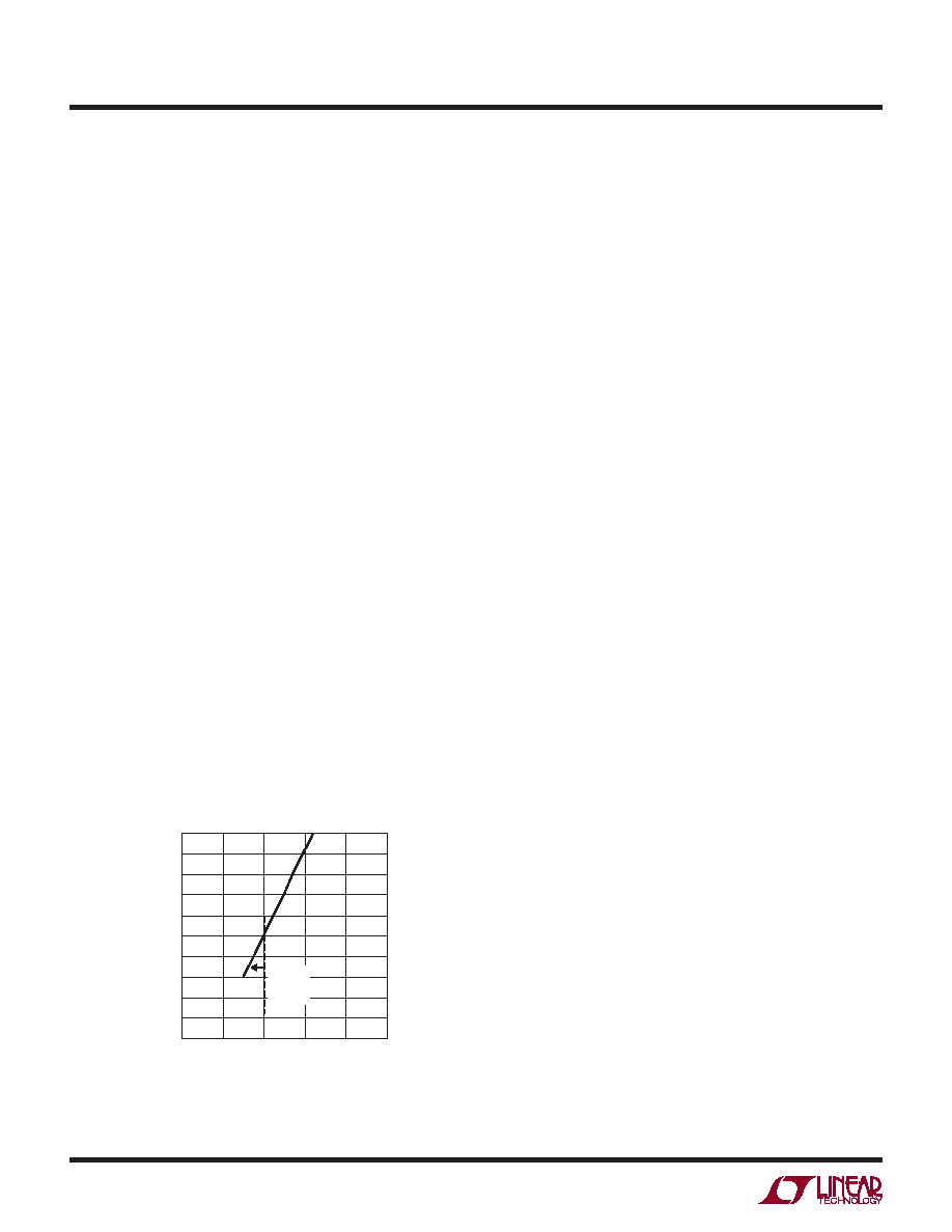
The LTC2453 includes a proprietary system that can,
typically, correctly digitize each input 8LSB above
VREF+ and below VREF–, if the LTC2453’s output is not
clamped. As an example (Figure 2), if the user desires to
measure a signal slightly below ground, the user could
set VIN– = VREF– = GND, and VREF+ = 5V. If VIN+ = GND,
the output code would be approximately 32768. If VIN+
= GND – 8LSB = –1.22 mV, the output code would be
approximately 32760.
The total amount of overrange and underrange capability
is typically 31LSB for a given device. The 31LSB total
is distributed between the overrange and underrange
capability. For example, if the underrange capability is
8LSB,theoverrangecapabilityistypically31–8=23LSB.
I2C INTERFACE
The LTC2453 communicates through an I2C interface. The
I2C interface is a 2-wire open-drain interface supporting
multiple devices and masters on a single bus. The con-
nected devices can only pull the data line (SDA) LOW and
never drive it HIGH. SDA must be externally connected to
the supply through a pull-up resistor. When the data line
is free, it is HIGH. Data on the I2C bus can be transferred
at rates up to 100kbits/s in the Standard-Mode and up to
400kbits/s in the Fast-Mode. The VCC power should not
be removed from the device when the I2C bus is active to
avoid loading the I2C bus lines through the internal ESD
protection diodes.
Each device on the I2C bus is recognized by a unique
address stored in that device and can operate either as
a transmitter or receiver, depending on the function of
the device. In addition to transmitters and receivers,
devices can also be considered as masters or slaves when
performing data transfers. A master is the device which
initiates a data transfer on the bus and generates the
clock signals to permit that transfer. Devices addressed
by the master are considered a slave. The address of the
LTC2453 is 0010100.
The LTC2453 can only be addressed as a slave. It can only
transmit the last conversion result. The serial clock line,
SCL, is always an input to the LTC2453 and the serial data
line SDA is bidirectional. Figure 3 shows the definition of
the I2C timing.
The START and STOP Conditions
A START (S) condition is generated by transitioning SDA
from HIGH to LOW while SCL is HIGH. The bus is consid-
ered to be busy after the START condition. When the data
transfer is finished, a STOP (P) condition is generated by
transitioning SDA from LOW to HIGH while SCL is HIGH.
The bus is free after a STOP is generated. START and STOP
conditions are always generated by the master.
When the bus is in use, it stays busy if a repeated START
(Sr)isgeneratedinsteadofaSTOPcondition.Therepeated
VIN+/VREF+
–0.001
OUTPUT
CODE
32772
32780
32788
0.001
2453 F02
32764
32756
32768
32776
32784
32760
32752
32748
–0.005
0
0.005
0.0015
SIGNALS
BELOW
GND
Figure 2. Output Code vs VIN+ with VIN– = 0 and VREF– = 0
APPLICATIONS INFORMATION
相关PDF资料 |
PDF描述 |
|---|---|
| VI-B0X-MX-F3 | CONVERTER MOD DC/DC 5.2V 75W |
| VI-B0X-MX-F2 | CONVERTER MOD DC/DC 5.2V 75W |
| VI-B0X-MX-F1 | CONVERTER MOD DC/DC 5.2V 75W |
| 97-3106A-22-19P | CONN PLUG 14POS W/PINS |
| MAX11644EUA+ | IC ADC 12BIT I2C/SRL 1CH 8UMAX |
相关代理商/技术参数 |
参数描述 |
|---|---|
| LTC2453ITS8#PBF | 制造商:Linear Technology 功能描述:ADC Single Delta-Sigma 60sps 16-bit Serial 8-Pin TSOT-23 制造商:Linear Technology 功能描述:Bulk |
| LTC2453ITS8#TRMPBF | 功能描述:IC ADC 16BIT DELTA SIG TSOT23-8 RoHS:是 类别:集成电路 (IC) >> 数据采集 - 模数转换器 系列:- 标准包装:2,500 系列:- 位数:16 采样率(每秒):15 数据接口:MICROWIRE?,串行,SPI? 转换器数目:1 功率耗散(最大):480µW 电压电源:单电源 工作温度:-40°C ~ 85°C 安装类型:表面贴装 封装/外壳:38-WFQFN 裸露焊盘 供应商设备封装:38-QFN(5x7) 包装:带卷 (TR) 输入数目和类型:16 个单端,双极;8 个差分,双极 配用:DC1011A-C-ND - BOARD DELTA SIGMA ADC LTC2494 |
| LTC2453ITS8#TRPBF | 功能描述:IC ADC 16BIT DELTA SIG TSOT23-8 RoHS:是 类别:集成电路 (IC) >> 数据采集 - 模数转换器 系列:- 标准包装:2,500 系列:- 位数:16 采样率(每秒):15 数据接口:MICROWIRE?,串行,SPI? 转换器数目:1 功率耗散(最大):480µW 电压电源:单电源 工作温度:-40°C ~ 85°C 安装类型:表面贴装 封装/外壳:38-WFQFN 裸露焊盘 供应商设备封装:38-QFN(5x7) 包装:带卷 (TR) 输入数目和类型:16 个单端,双极;8 个差分,双极 配用:DC1011A-C-ND - BOARD DELTA SIGMA ADC LTC2494 |
| LTC2460CDD#PBF | 功能描述:IC ADC 16BIT DELTA SIG 12-DFN RoHS:是 类别:集成电路 (IC) >> 数据采集 - 模数转换器 系列:- 标准包装:1 系列:microPOWER™ 位数:8 采样率(每秒):1M 数据接口:串行,SPI? 转换器数目:1 功率耗散(最大):- 电压电源:模拟和数字 工作温度:-40°C ~ 125°C 安装类型:表面贴装 封装/外壳:24-VFQFN 裸露焊盘 供应商设备封装:24-VQFN 裸露焊盘(4x4) 包装:Digi-Reel® 输入数目和类型:8 个单端,单极 产品目录页面:892 (CN2011-ZH PDF) 其它名称:296-25851-6 |
| LTC2460CDD#TRPBF | 功能描述:IC ADC 16BIT DELTA SIG 12-DFN RoHS:是 类别:集成电路 (IC) >> 数据采集 - 模数转换器 系列:- 标准包装:2,500 系列:- 位数:16 采样率(每秒):15 数据接口:MICROWIRE?,串行,SPI? 转换器数目:1 功率耗散(最大):480µW 电压电源:单电源 工作温度:-40°C ~ 85°C 安装类型:表面贴装 封装/外壳:38-WFQFN 裸露焊盘 供应商设备封装:38-QFN(5x7) 包装:带卷 (TR) 输入数目和类型:16 个单端,双极;8 个差分,双极 配用:DC1011A-C-ND - BOARD DELTA SIGMA ADC LTC2494 |
发布紧急采购,3分钟左右您将得到回复。