- 您现在的位置:买卖IC网 > PDF目录10502 > LTC2453IDDB#TRMPBF (Linear Technology)IC ADC 16BIT DELTA SIG 8-DFN PDF资料下载
参数资料
| 型号: | LTC2453IDDB#TRMPBF |
| 厂商: | Linear Technology |
| 文件页数: | 18/18页 |
| 文件大小: | 0K |
| 描述: | IC ADC 16BIT DELTA SIG 8-DFN |
| 产品培训模块: | LTC2460 and LTC2450 Delta Sigma ADC Families |
| 标准包装: | 1 |
| 位数: | 16 |
| 采样率(每秒): | 60 |
| 数据接口: | I²C,串行 |
| 转换器数目: | 2 |
| 功率耗散(最大): | 4mW |
| 电压电源: | 单电源 |
| 工作温度: | -40°C ~ 85°C |
| 安装类型: | 表面贴装 |
| 封装/外壳: | 8-WFDFN 裸露焊盘 |
| 供应商设备封装: | 8-DFN(3x2) |
| 包装: | 标准包装 |
| 输入数目和类型: | 1 个差分,双极 |
| 产品目录页面: | 1348 (CN2011-ZH PDF) |
| 其它名称: | LTC2453IDDB#TRMPBFDKR |
LTC2453
9
2453fc
START timing is functionally identical to the START and
is used for reading from the device before the initiation
of a new conversion.
Data Transferring
After the START condition, the I2C bus is busy and data
transfer can begin between the master and the addressed
slave. Data is transferred over the bus in groups of nine
bits, one byte followed by one acknowledge (ACK) bit. The
master releases the SDA line during the ninth SCL clock
cycle. The slave device can issue an ACK by pulling SDA
LOW or issue a Not Acknowledge (NAK) by leaving the
SDA line HIGH impedance (the external pull-up resistor
will hold the line HIGH). Change of data only occurs while
the clock line (SCL) is LOW.
Data Format
After a START condition, the master sends a 7-bit address
followed by a read request (R) bit. The bit R is 1 for a
Read Request. If the 7-bit address matches the LTC2453’s
address (hard-wired at 0010100) the ADC is selected.
When the device is addressed during the conversion
state, it does not accept the request and issues a NAK by
leaving the SDA line HIGH. If the conversion is complete,
the LTC2453 issues an ACK by pulling the SDA line LOW.
Following the ACK, the LTC2453 can output data. The data
output stream is 16 bits long and is shifted out on the
falling edges of SCL (see Figure 4). The first bit output by
the LTC2453, the MSB, is the sign, which is 1 for VIN+ ≥
VIN– and 0 for VIN+ < VIN– (see Table 1). The MSB (D15) is
followedbysuccessivelylesssignificantbits(D14,D13…)
until the LSB is output by the LTC2453. This sequence is
shown in Figure 5.
OPERATION SEQUENCE
Continuous Read
Conversions from the LTC2453 can be continuously
read, see Figure 6. At the end of a read operation, a new
conversion automatically begins. At the conclusion of
the conversion cycle, the next result may be read using
the method described above. If the conversion cycle is
not complete and a valid address selects the device, the
LTC2453 generates a NAK signal indicating the conversion
cycle is in progress.
Discarding a Conversion Result and Initiating a New
Conversion
It is possible to start a new conversion without reading
the old result, as shown in Figure 7. Following a valid 7-bit
address, a read request (R) bit, and a valid ACK, a STOP
command will start a new conversion.
PRESERVING THE CONVERTER ACCURACY
TheLTC2453isdesignedtodramaticallyreducetheconver-
sion result’s sensitivity to device decoupling, PCB layout,
antialiasing circuits, line and frequency perturbations.
Nevertheless, in order to preserve the high accuracy capa-
bility of this part, some simple precautions are desirable.
Digital Signal Levels
Due to the nature of CMOS logic, it is advisable to keep
input digital signals near GND or VCC. Voltages in the
range of 0.5V to VCC – 0.5V may result in additional cur-
rent leakage from the part.
SDA
SCL
S
Sr
P
S
tHD(STA)
tHD(DAT)
tSU(STA)
tSU(STO)
tSU(DAT)
tLOW
tHD(SDA)
tSP
tBUF
tr
tf
tr
tf
tHIGH
2453 F03
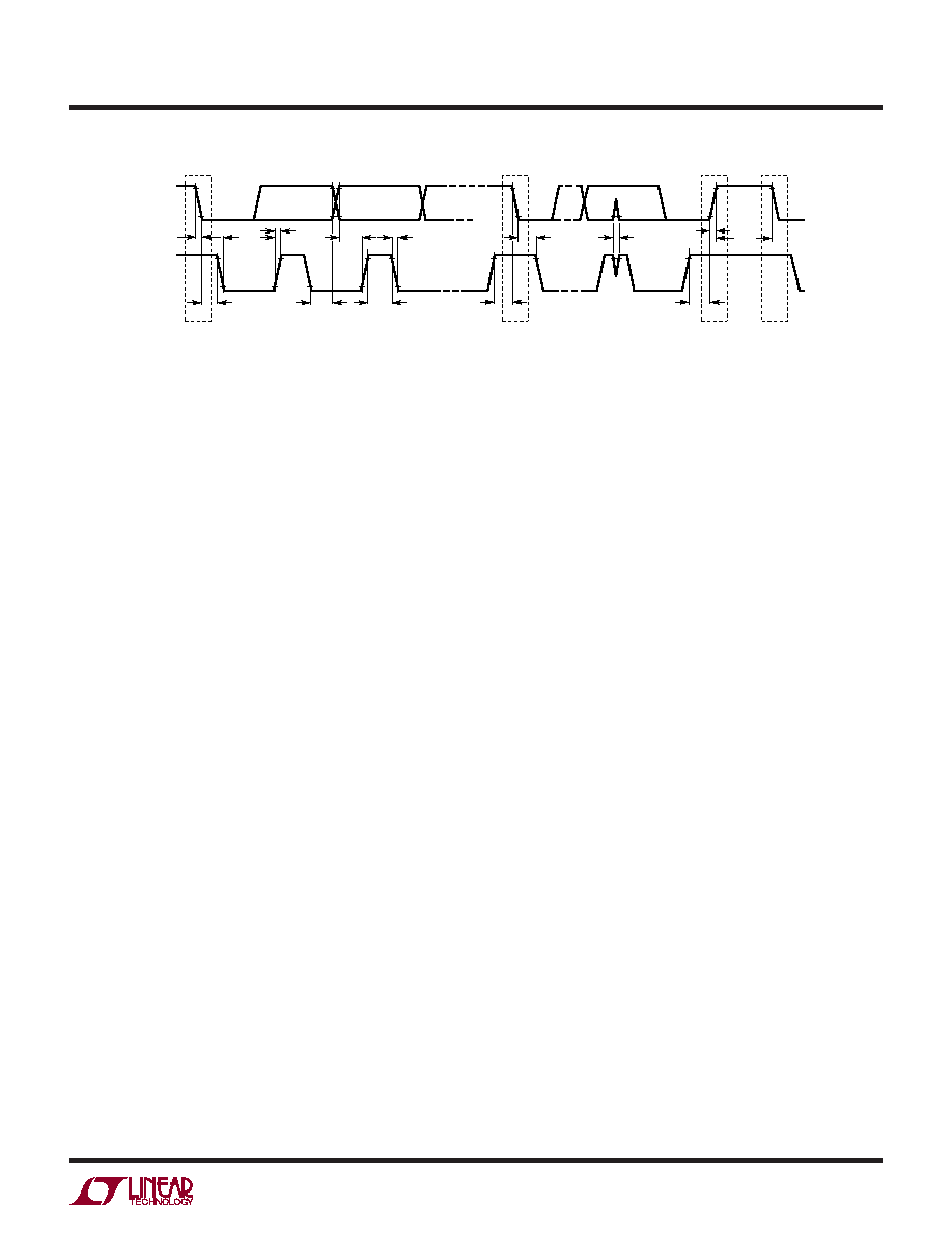
Figure 3. Definition of Timing for Fast/Standard Mode Devices on the I2C Bus
APPLICATIONS INFORMATION
相关PDF资料 |
PDF描述 |
|---|---|
| VI-B0X-MX-F3 | CONVERTER MOD DC/DC 5.2V 75W |
| VI-B0X-MX-F2 | CONVERTER MOD DC/DC 5.2V 75W |
| VI-B0X-MX-F1 | CONVERTER MOD DC/DC 5.2V 75W |
| 97-3106A-22-19P | CONN PLUG 14POS W/PINS |
| MAX11644EUA+ | IC ADC 12BIT I2C/SRL 1CH 8UMAX |
相关代理商/技术参数 |
参数描述 |
|---|---|
| LTC2453ITS8#PBF | 制造商:Linear Technology 功能描述:ADC Single Delta-Sigma 60sps 16-bit Serial 8-Pin TSOT-23 制造商:Linear Technology 功能描述:Bulk |
| LTC2453ITS8#TRMPBF | 功能描述:IC ADC 16BIT DELTA SIG TSOT23-8 RoHS:是 类别:集成电路 (IC) >> 数据采集 - 模数转换器 系列:- 标准包装:2,500 系列:- 位数:16 采样率(每秒):15 数据接口:MICROWIRE?,串行,SPI? 转换器数目:1 功率耗散(最大):480µW 电压电源:单电源 工作温度:-40°C ~ 85°C 安装类型:表面贴装 封装/外壳:38-WFQFN 裸露焊盘 供应商设备封装:38-QFN(5x7) 包装:带卷 (TR) 输入数目和类型:16 个单端,双极;8 个差分,双极 配用:DC1011A-C-ND - BOARD DELTA SIGMA ADC LTC2494 |
| LTC2453ITS8#TRPBF | 功能描述:IC ADC 16BIT DELTA SIG TSOT23-8 RoHS:是 类别:集成电路 (IC) >> 数据采集 - 模数转换器 系列:- 标准包装:2,500 系列:- 位数:16 采样率(每秒):15 数据接口:MICROWIRE?,串行,SPI? 转换器数目:1 功率耗散(最大):480µW 电压电源:单电源 工作温度:-40°C ~ 85°C 安装类型:表面贴装 封装/外壳:38-WFQFN 裸露焊盘 供应商设备封装:38-QFN(5x7) 包装:带卷 (TR) 输入数目和类型:16 个单端,双极;8 个差分,双极 配用:DC1011A-C-ND - BOARD DELTA SIGMA ADC LTC2494 |
| LTC2460CDD#PBF | 功能描述:IC ADC 16BIT DELTA SIG 12-DFN RoHS:是 类别:集成电路 (IC) >> 数据采集 - 模数转换器 系列:- 标准包装:1 系列:microPOWER™ 位数:8 采样率(每秒):1M 数据接口:串行,SPI? 转换器数目:1 功率耗散(最大):- 电压电源:模拟和数字 工作温度:-40°C ~ 125°C 安装类型:表面贴装 封装/外壳:24-VFQFN 裸露焊盘 供应商设备封装:24-VQFN 裸露焊盘(4x4) 包装:Digi-Reel® 输入数目和类型:8 个单端,单极 产品目录页面:892 (CN2011-ZH PDF) 其它名称:296-25851-6 |
| LTC2460CDD#TRPBF | 功能描述:IC ADC 16BIT DELTA SIG 12-DFN RoHS:是 类别:集成电路 (IC) >> 数据采集 - 模数转换器 系列:- 标准包装:2,500 系列:- 位数:16 采样率(每秒):15 数据接口:MICROWIRE?,串行,SPI? 转换器数目:1 功率耗散(最大):480µW 电压电源:单电源 工作温度:-40°C ~ 85°C 安装类型:表面贴装 封装/外壳:38-WFQFN 裸露焊盘 供应商设备封装:38-QFN(5x7) 包装:带卷 (TR) 输入数目和类型:16 个单端,双极;8 个差分,双极 配用:DC1011A-C-ND - BOARD DELTA SIGMA ADC LTC2494 |
发布紧急采购,3分钟左右您将得到回复。