- 您现在的位置:买卖IC网 > PDF目录10689 > LTC2489IDE#PBF (Linear Technology)IC ADC 16BIT DELTA SIG 14-DFN PDF资料下载
参数资料
| 型号: | LTC2489IDE#PBF |
| 厂商: | Linear Technology |
| 文件页数: | 3/24页 |
| 文件大小: | 0K |
| 描述: | IC ADC 16BIT DELTA SIG 14-DFN |
| 标准包装: | 91 |
| 位数: | 16 |
| 采样率(每秒): | 7.5 |
| 数据接口: | I²C,串行 |
| 转换器数目: | 1 |
| 功率耗散(最大): | 480µW |
| 电压电源: | 单电源 |
| 工作温度: | -40°C ~ 85°C |
| 安装类型: | 表面贴装 |
| 封装/外壳: | 14-WFDFN 裸露焊盘 |
| 供应商设备封装: | 14-DFN-EP(4x3) |
| 包装: | 管件 |
| 输入数目和类型: | 4 个单端,双极;2 个差分,双极 |
| 产品目录页面: | 1348 (CN2011-ZH PDF) |
| 配用: | DC1010A-B-ND - BOARD DELTA SIGMA ADC LTC2489 |
LTC2489
11
2489fa
The Start and Stop Conditions
A Start (S) condition is generated by transitioning SDA from
high to low while SCL is high. The bus is considered to be
busy after the Start condition. When the data transfer is
finished, a Stop (P) condition is generated by transitioning
SDA from low to high while SCL is high. The bus is free
after a Stop is generated. Start and Stop conditions are
always generated by the master.
When the bus is in use, it stays busy if a Repeated Start
(Sr) is generated instead of a Stop condition. The repeated
Start timing is functionally identical to the Start and is
used for writing and reading from the device before the
initiation of a new conversion.
Data Transferring
After the Start condition, the I2C bus is busy and data
transfer can begin between the master and the addressed
slave. Data is transferred over the bus in groups of nine
bits, one byte followed by one acknowledge (ACK) bit.
The master releases the SDA line during the ninth SCL
clock cycle. The slave device can issue an ACK by pulling
SDA low or issue a Not Acknowledge (NAK) by leaving
the SDA line high impedance (the external pull-up resistor
will hold the line high). Change of data only occurs while
the clock line (SCL) is low.
DATA FORMAT
After a Start condition, the master sends a 7-bit address
followed by a read/write (R/W) bit. The R/W bit is 1 for
a read request and 0 for a write request. If the 7-bit ad-
dress matches the hard wired, LTC2489’s address (one of
9 pin-selectable addresses) the device is selected. When
the device is addressed during the conversion state, it will
not acknowledge R/W requests and will issue a NAK by
leaving the SDA line high. If the conversion is complete,
the LTC2489 issues an ACK by pulling the SDA line low.
The LTC2489 has two registers. The output register (24
bits long) contains the last conversion result. The input
register (8 bits long) sets the input channel.
DATA OUTPUT FORMAT
The output register contains the last conversion result.
After each conversion is completed, the device automati-
cally enters the sleep state where the supply current is
reduced to 1μA. When the LTC2489 is addressed for a read
operation, it acknowledges (by pulling SDA low) and acts
as a transmitter. The master/receiver can read up to three
bytes from the LTC2489. After a complete read operation
(3 bytes), a new conversion is initiated. The device will
NAK subsequent read operations while a conversion is
being performed.
The data output stream is 24 bits long and is shifted out
on the falling edges of SCL (see Figure 3a). The first bit
is the conversion result sign bit (SIG) (see Tables 1 and
2). This bit is high if VIN ≥ 0 and low if VIN < 0 (where VIN
corresponds to the selected input signal IN+ – IN–). The
second bit is the most significant bit (MSB) of the result.
The first two bits (SIG and MSB) can be used to indicate
over and under range conditions (see Table 2). If both bits
are HIGH, the differential input voltage is equal to or above
+FS. If both bits are set low, the input voltage is below
–FS. The function of these bits is summarized in Table 2.
The 16 bits following the MSB bit are the conversion
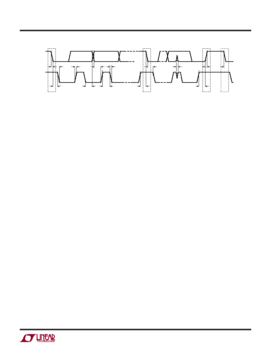
SDA
SCL
SSr
P
S
tHD(SDA)
tHD(DAT)
tSU(STA)
tSU(STO)
tSU(DAT)
tLOW
tHD(SDA)
tSP
tBUF
tr
tf
tr
tf
tHIGH
2489 F02
Figure 2. Definition of Timing for Fast/Standard Mode Devices on the I2C Bus
APPLICATIONS INFORMATION
相关PDF资料 |
PDF描述 |
|---|---|
| LT1017CSW#PBF | IC COMPARATOR MCRPWR DUAL 16SOIC |
| ISL31483EIBZ-T7A | IC TXRX RS485 FAULT PROT 14SOIC |
| VE-23Y-MX-B1 | CONVERTER MOD DC/DC 3.3V 49.5W |
| LT1017CSW | IC COMPARATOR MCRPWR DUAL 16SOIC |
| LTC1197IS8#PBF | IC A/DCONV 10BIT W/SHTDWN 8-SOIC |
相关代理商/技术参数 |
参数描述 |
|---|---|
| LTC2492CDE | 制造商:Linear Technology 功能描述:ADC Single Delta-Sigma 7.5sps 24-bit Serial 14-Pin DFN EP |
| LTC2492CDE#PBF | 功能描述:IC ADC 24BIT DELTA SIG 14-DFN RoHS:是 类别:集成电路 (IC) >> 数据采集 - 模数转换器 系列:- 标准包装:1 系列:microPOWER™ 位数:8 采样率(每秒):1M 数据接口:串行,SPI? 转换器数目:1 功率耗散(最大):- 电压电源:模拟和数字 工作温度:-40°C ~ 125°C 安装类型:表面贴装 封装/外壳:24-VFQFN 裸露焊盘 供应商设备封装:24-VQFN 裸露焊盘(4x4) 包装:Digi-Reel® 输入数目和类型:8 个单端,单极 产品目录页面:892 (CN2011-ZH PDF) 其它名称:296-25851-6 |
| LTC2492CDE#TRPBF | 功能描述:IC ADC 24BIT DELTA SIG 14-DFN RoHS:是 类别:集成电路 (IC) >> 数据采集 - 模数转换器 系列:- 标准包装:2,500 系列:- 位数:16 采样率(每秒):15 数据接口:MICROWIRE?,串行,SPI? 转换器数目:1 功率耗散(最大):480µW 电压电源:单电源 工作温度:-40°C ~ 85°C 安装类型:表面贴装 封装/外壳:38-WFQFN 裸露焊盘 供应商设备封装:38-QFN(5x7) 包装:带卷 (TR) 输入数目和类型:16 个单端,双极;8 个差分,双极 配用:DC1011A-C-ND - BOARD DELTA SIGMA ADC LTC2494 |
| LTC2492IDE#PBF | 功能描述:IC ADC 24BIT DELTA SIG 14-DFN RoHS:是 类别:集成电路 (IC) >> 数据采集 - 模数转换器 系列:- 标准包装:1 系列:microPOWER™ 位数:8 采样率(每秒):1M 数据接口:串行,SPI? 转换器数目:1 功率耗散(最大):- 电压电源:模拟和数字 工作温度:-40°C ~ 125°C 安装类型:表面贴装 封装/外壳:24-VFQFN 裸露焊盘 供应商设备封装:24-VQFN 裸露焊盘(4x4) 包装:Digi-Reel® 输入数目和类型:8 个单端,单极 产品目录页面:892 (CN2011-ZH PDF) 其它名称:296-25851-6 |
| LTC2492IDE#TRPBF | 功能描述:IC ADC 24BIT DELTA SIG 14-DFN RoHS:是 类别:集成电路 (IC) >> 数据采集 - 模数转换器 系列:- 标准包装:1,000 系列:- 位数:16 采样率(每秒):45k 数据接口:串行 转换器数目:2 功率耗散(最大):315mW 电压电源:模拟和数字 工作温度:0°C ~ 70°C 安装类型:表面贴装 封装/外壳:28-SOIC(0.295",7.50mm 宽) 供应商设备封装:28-SOIC W 包装:带卷 (TR) 输入数目和类型:2 个单端,单极 |
发布紧急采购,3分钟左右您将得到回复。