- 您现在的位置:买卖IC网 > PDF目录8661 > LTC2607IDE-1#TRPBF (Linear Technology)IC DAC 16BIT R-R I2C 12-DFN PDF资料下载
参数资料
| 型号: | LTC2607IDE-1#TRPBF |
| 厂商: | Linear Technology |
| 文件页数: | 16/20页 |
| 文件大小: | 0K |
| 描述: | IC DAC 16BIT R-R I2C 12-DFN |
| 标准包装: | 2,500 |
| 设置时间: | 10µs |
| 位数: | 16 |
| 数据接口: | I²C |
| 转换器数目: | 2 |
| 电压电源: | 单电源 |
| 功率耗散(最大): | 780µW |
| 工作温度: | -40°C ~ 85°C |
| 安装类型: | 表面贴装 |
| 封装/外壳: | 12-WFDFN 裸露焊盘 |
| 供应商设备封装: | 12-DFN(4x3) |
| 包装: | 带卷 (TR) |
| 输出数目和类型: | 2 电压,单极 |
| 采样率(每秒): | * |
| 配用: | DC934A-ND - BOARD DAC LTC2607 |
LTC2607/LTC2617/LTC2627
26071727fa
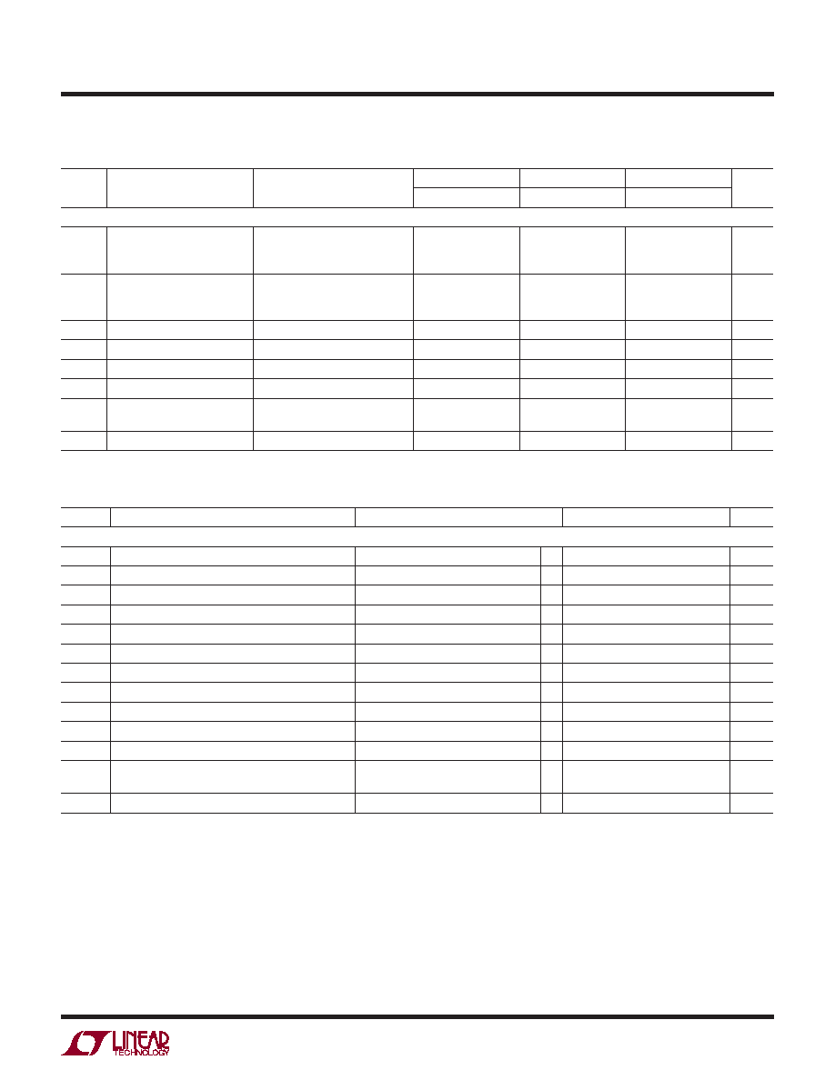
electrical characteristics
timing characteristics
Note 1: Stresses beyond those listed under Absolute Maximum Ratings
may cause permanent damage to the device. Exposure to any Absolute
Maximum Rating condition for extended periods may affect device
reliability and lifetime.
Note 2: Linearity and monotonicity are defined from code kL to code
2N – 1, where N is the resolution and kL is given by kL = 0.016(2N/VREF),
rounded to the nearest whole code. For VREF = 4.096V and N = 16, kL =
256 and linearity is defined from code 256 to code 65,535.
Note 3: SDA, SCL and LDAC at 0V or VCC, CA0, CA1 and CA2 Floating.
Note 4: DC crosstalk is measured with VCC = 5V and VREF = 4.096V, with
the measured DAC at mid-scale, unless otherwise noted.
SYMBOL PARAMETER
CONDITIONS
MIN
TYP
MAX
UNITS
VCC = 2.7V to 5.5V
fSCL
SCL Clock Frequency
l
0
400
kHz
tHD(STA)
Hold Time (Repeated) Start Condition
l
0.6
s
tLOW
Low Period of the SCL Clock Pin
l
1.3
s
tHIGH
High Period of the SCL Clock Pin
l
0.6
s
tSU(STA)
Set-Up Time for a Repeated Start Condition
l
0.6
s
tHD(DAT)
Data Hold Time
l
0
0.9
s
tSU(DAT)
Data Set-Up Time
l
100
ns
tr
Rise Time of Both SDA and SCL Signals
(Note 9)
l
20 + 0.1CB
300
ns
tf
Fall Time of Both SDA and SCL Signals
(Note 9)
l
20 + 0.1CB
300
ns
tSU(STO)
Set-Up Time for Stop Condition
l
0.6
s
tBUF
Bus Free Time Between a Stop and Start Condition
l
1.3
s
t1
Falling Edge of 9th Clock of the 3rd Input Byte to
LDAC High or Low Transition
l
400
ns
t2
LDAC Low Pulse Width
l
20
ns
The l denotes the specifications which apply over the full operating temperature
range, otherwise specifications are at TA = 25°C. (See Figure 1) (Notes 10, 11)
The l denotes the specifications which apply over the full operating
temperature range, otherwise specifications are at TA = 25°C. REF = 4.096V (VCC = 5V), REF = 2.048V (VCC = 2.7V), REFLO = 0V,
VOUT unloaded, unless otherwise noted.
SYMBOL PARAMETER
CONDITIONS
LTC2627/LTC2627-1 LTC2617/LTC2617-1 LTC2607/LTC2607-1
UNITS
MIN
TYP MAX MIN
TYP MAX
AC Performance
tS
Settling Time (Note 7)
±0.024% (±1LSB at 12 Bits)
±0.006% (±1LSB at 14 Bits)
±0.0015% (±1LSB at 16 Bits)
7
9
7
9
10
s
Settling Time for 1LSB Step
(Note 8)
±0.024% (±1LSB at 12 Bits)
±0.006% (±1LSB at 14 Bits)
±0.0015% (±1LSB at 16 Bits)
2.7
4.8
2.7
4.8
5.2
s
Voltage Output Slew Rate
0.8
V/s
Capacitive Load Driving
1000
pF
Glitch Impulse
At Mid-Scale Transition
12
nV s
Multiplying Bandwidth
180
kHz
en
Output Voltage Noise Density At f = 1kHz
At f = 10kHz
120
100
120
100
120
100
nV/√Hz
Output Voltage Noise
0.1Hz to 10Hz
15
VP-P
Note 5: RL = 2kΩ to GND or VCC.
Note 6: Inferred from measurement at code kL (Note 2) and at full scale.
Note 7: VCC = 5V, VREF = 4.096V. DAC is stepped 1/4 scale to 3/4 scale
and 3/4 scale to 1/4 scale. Load is 2k in parallel with 200pF to GND.
Note 8: VCC = 5V, VREF = 4.096V. DAC is stepped ±1LSB between half
scale and half scale – 1. Load is 2k in parallel with 200pF to GND.
Note 9: CB = capacitance of one bus line in pF.
Note 10: All values refer to VIH(MIN) and VIL(MAX) levels.
Note 11: These specifications apply to LTC2607/LTC2607-1,
LTC2617/LTC2617-1, LTC2627/LTC2627-1.
Note 12: Guaranteed by design and not production tested.
相关PDF资料 |
PDF描述 |
|---|---|
| VE-J23-MY | CONVERTER MOD DC/DC 24V 50W |
| VE-J22-MY | CONVERTER MOD DC/DC 15V 50W |
| AD8802ARZ | IC DAC 8BIT 12CH W/SD 20SOIC |
| VI-JWZ-MW | CONVERTER MOD DC/DC 2V 40W |
| VI-JWY-MY | CONVERTER MOD DC/DC 3.3V 33W |
相关代理商/技术参数 |
参数描述 |
|---|---|
| LTC2609CGN#PBF | 功能描述:IC DAC 16BIT R-R QUAD 16SSOP RoHS:是 类别:集成电路 (IC) >> 数据采集 - 数模转换器 系列:- 产品培训模块:Data Converter Fundamentals DAC Architectures 标准包装:750 系列:- 设置时间:7µs 位数:16 数据接口:并联 转换器数目:1 电压电源:双 ± 功率耗散(最大):100mW 工作温度:0°C ~ 70°C 安装类型:表面贴装 封装/外壳:28-LCC(J 形引线) 供应商设备封装:28-PLCC(11.51x11.51) 包装:带卷 (TR) 输出数目和类型:1 电压,单极;1 电压,双极 采样率(每秒):143k |
| LTC2609CGN#TRPBF | 功能描述:IC DAC 16BIT R-R QUAD 16SSOP RoHS:是 类别:集成电路 (IC) >> 数据采集 - 数模转换器 系列:- 标准包装:2,400 系列:- 设置时间:- 位数:18 数据接口:串行 转换器数目:3 电压电源:模拟和数字 功率耗散(最大):- 工作温度:-40°C ~ 85°C 安装类型:表面贴装 封装/外壳:36-TFBGA 供应商设备封装:36-TFBGA 包装:带卷 (TR) 输出数目和类型:* 采样率(每秒):* |
| LTC2609CGN-1#PBF | 功能描述:IC DAC 16BIT R-R QUAD 16SSOP RoHS:是 类别:集成电路 (IC) >> 数据采集 - 数模转换器 系列:- 标准包装:47 系列:- 设置时间:2µs 位数:14 数据接口:并联 转换器数目:1 电压电源:单电源 功率耗散(最大):55µW 工作温度:-40°C ~ 85°C 安装类型:表面贴装 封装/外壳:28-SSOP(0.209",5.30mm 宽) 供应商设备封装:28-SSOP 包装:管件 输出数目和类型:1 电流,单极;1 电流,双极 采样率(每秒):* |
| LTC2609CGN-1#TRPBF | 功能描述:IC DAC 16BIT R-R QUAD 16SSOP RoHS:是 类别:集成电路 (IC) >> 数据采集 - 数模转换器 系列:- 标准包装:2,400 系列:- 设置时间:- 位数:18 数据接口:串行 转换器数目:3 电压电源:模拟和数字 功率耗散(最大):- 工作温度:-40°C ~ 85°C 安装类型:表面贴装 封装/外壳:36-TFBGA 供应商设备封装:36-TFBGA 包装:带卷 (TR) 输出数目和类型:* 采样率(每秒):* |
| LTC2609IGN#PBF | 功能描述:IC DAC 16BIT R-R QUAD 16SSOP RoHS:是 类别:集成电路 (IC) >> 数据采集 - 数模转换器 系列:- 产品培训模块:Data Converter Fundamentals DAC Architectures 标准包装:750 系列:- 设置时间:7µs 位数:16 数据接口:并联 转换器数目:1 电压电源:双 ± 功率耗散(最大):100mW 工作温度:0°C ~ 70°C 安装类型:表面贴装 封装/外壳:28-LCC(J 形引线) 供应商设备封装:28-PLCC(11.51x11.51) 包装:带卷 (TR) 输出数目和类型:1 电压,单极;1 电压,双极 采样率(每秒):143k |
发布紧急采购,3分钟左右您将得到回复。