参数资料
| 型号: | LTC2627IDE#PBF |
| 厂商: | Linear Technology |
| 文件页数: | 7/20页 |
| 文件大小: | 0K |
| 描述: | IC DAC 12BIT R-R I2C 12-DFN |
| 标准包装: | 91 |
| 设置时间: | 7µs |
| 位数: | 12 |
| 数据接口: | I²C |
| 转换器数目: | 2 |
| 电压电源: | 单电源 |
| 功率耗散(最大): | 780µW |
| 工作温度: | -40°C ~ 85°C |
| 安装类型: | 表面贴装 |
| 封装/外壳: | 12-WFDFN 裸露焊盘 |
| 供应商设备封装: | 12-DFN(4x3) |
| 包装: | 管件 |
| 输出数目和类型: | 2 电压,单极 |
| 采样率(每秒): | * |
| 产品目录页面: | 1351 (CN2011-ZH PDF) |
LTC2607/LTC2617/LTC2627
26071727fa
operation
Table 2
COMMAND*
C3
C2
C1
C0
0
0 Write to Input Register
0
1 Update (Power Up) DAC Register
0
1
1 Write to and Update (Power Up)
0
1
0
0 Power Down
1
1 No Operation
ADDRESS*
A3
A2
A1
A0
0
0 DAC A
0
1 DAC B
1
1 All DACs
*Command and address codes not shown are reserved and should not be used.
Power-Down Mode
Forpower-constrainedapplications,thepower-downmode
can be used to reduce the supply current whenever one or
both of the DAC outputs are not needed. When in power-
down,thebufferamplifiers,biascircuitsandreferenceinput
are disabled and draw essentially zero current. The DAC
outputsareputintoahighimpedancestate,andtheoutput
pins are passively pulled to VREFLO through 90k resistors.
Input-registerandDAC-registercontentsarenotdisturbed
during power-down.
Either or both DAC channels can be put into power-down
mode by using command 0100b in combination with the
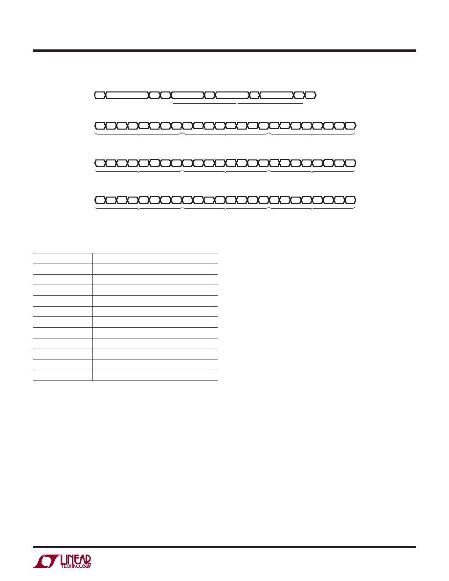
Figure 3
C3
1ST DATA BYTE
Input Word (LTC2607)
Write Word Protocol for LTC2607/LTC2617/LTC1627
C2 C1 C0 A3 A2 A1 A0
D13
D14
D15
S
W
A
SLAVE ADDRESS
1ST DATA BYTE
D12 D11 D10 D9 D8 D7 D6 D5 D4 D3 D2 D1 D0
A
2ND DATA BYTE
A 3RD DATA BYTE
A
P
2607 F03
2ND DATA BYTE
INPUT WORD
3RD DATA BYTE
C3
1ST DATA BYTE
Input Word (LTC2617)
C2 C1 C0 A3 A2 A1 A0
D11
D12
D13
D10 D9 D8 D7 D6 D5 D4 D3 D2 D1 D0
X
2ND DATA BYTE
3RD DATA BYTE
C3
1ST DATA BYTE
Input Word (LTC2627)
C2 C1 C0 A3 A2 A1 A0
D9
D10
D11
D8 D7 D6 D5 D4 D3 D2 D1 D0
X
2ND DATA BYTE
3RD DATA BYTE
appropriate DAC address. The 16-bit data word is ignored.
The supply and reference currents are reduced by approxi-
mately 50% for each DAC powered down; the effective
resistance at REF (Pin 9) rises accordingly, becoming a
high-impedance input (typically > 1GΩ) when both DACs
are powered down.
Normal operation can be resumed by executing any
command which includes a DAC update, as shown in
Table 2 or performing an asychronous update (LDAC) as
describedinthenextsection.TheselectedDACispowered
upasitsvoltageoutputisupdated.WhenaDACinpowered-
down state is powered up and updated, normal settling
is delayed. If one of the two DACs is in a powered- down
state prior to the update command, the power up delay is
5s. If on the other hand, both DACs are powered down,
the main bias generation circuit has been automatically
shut down in addition to the DAC amplifiers and reference
input and so the power up delay time is
12s (for VCC = 5V) or 30s (for VCC = 3V)
Asynchronous DAC Update Using LDAC
In addition to the update commands shown in Table 2, the
LDAC pin asynchronously updates the DAC registers with
the contents of the input registers. Asynchronous update
is disabled when the input word is being clocked into
the part.
相关PDF资料 |
PDF描述 |
|---|---|
| MS3451W28-15S | CONN RCPT 35POS CBL MNT W/SCKT |
| MS3451L28-15S | CONN RCPT 35POS CBL MNT W/SCKT |
| AD5334BRUZ | IC DAC 8BIT QUAD VOUT 24-TSSOP |
| VE-J4M-MZ-F3 | CONVERTER MOD DC/DC 10V 25W |
| LTC2627IDE-1#PBF | IC DAC 12BIT R-R I2C 12-DFN |
相关代理商/技术参数 |
参数描述 |
|---|---|
| LTC2629CGN#PBF | 功能描述:IC DAC 12BIT R-R QUAD 16SSOP RoHS:是 类别:集成电路 (IC) >> 数据采集 - 数模转换器 系列:- 产品培训模块:Lead (SnPb) Finish for COTS Obsolescence Mitigation Program 标准包装:50 系列:- 设置时间:4µs 位数:12 数据接口:串行 转换器数目:2 电压电源:单电源 功率耗散(最大):- 工作温度:-40°C ~ 85°C 安装类型:表面贴装 封装/外壳:8-TSSOP,8-MSOP(0.118",3.00mm 宽) 供应商设备封装:8-uMAX 包装:管件 输出数目和类型:2 电压,单极 采样率(每秒):* 产品目录页面:1398 (CN2011-ZH PDF) |
| LTC2629CGN#TRPBF | 功能描述:IC DAC 12BIT R-R QUAD 16SSOP RoHS:是 类别:集成电路 (IC) >> 数据采集 - 数模转换器 系列:- 标准包装:2,400 系列:- 设置时间:- 位数:18 数据接口:串行 转换器数目:3 电压电源:模拟和数字 功率耗散(最大):- 工作温度:-40°C ~ 85°C 安装类型:表面贴装 封装/外壳:36-TFBGA 供应商设备封装:36-TFBGA 包装:带卷 (TR) 输出数目和类型:* 采样率(每秒):* |
| LTC2629CGN-1#PBF | 功能描述:IC DAC 12BIT R-R QUAD 16SSOP RoHS:是 类别:集成电路 (IC) >> 数据采集 - 数模转换器 系列:- 产品培训模块:Lead (SnPb) Finish for COTS Obsolescence Mitigation Program 标准包装:50 系列:- 设置时间:4µs 位数:12 数据接口:串行 转换器数目:2 电压电源:单电源 功率耗散(最大):- 工作温度:-40°C ~ 85°C 安装类型:表面贴装 封装/外壳:8-TSSOP,8-MSOP(0.118",3.00mm 宽) 供应商设备封装:8-uMAX 包装:管件 输出数目和类型:2 电压,单极 采样率(每秒):* 产品目录页面:1398 (CN2011-ZH PDF) |
| LTC2629CGN-1#TRPBF | 功能描述:IC DAC 12BIT R-R QUAD 16SSOP RoHS:是 类别:集成电路 (IC) >> 数据采集 - 数模转换器 系列:- 标准包装:47 系列:- 设置时间:2µs 位数:14 数据接口:并联 转换器数目:1 电压电源:单电源 功率耗散(最大):55µW 工作温度:-40°C ~ 85°C 安装类型:表面贴装 封装/外壳:28-SSOP(0.209",5.30mm 宽) 供应商设备封装:28-SSOP 包装:管件 输出数目和类型:1 电流,单极;1 电流,双极 采样率(每秒):* |
| LTC2629IGN#PBF | 功能描述:IC DAC 12BIT R-R QUAD 16SSOP RoHS:是 类别:集成电路 (IC) >> 数据采集 - 数模转换器 系列:- 产品培训模块:Lead (SnPb) Finish for COTS Obsolescence Mitigation Program 标准包装:50 系列:- 设置时间:4µs 位数:12 数据接口:串行 转换器数目:2 电压电源:单电源 功率耗散(最大):- 工作温度:-40°C ~ 85°C 安装类型:表面贴装 封装/外壳:8-TSSOP,8-MSOP(0.118",3.00mm 宽) 供应商设备封装:8-uMAX 包装:管件 输出数目和类型:2 电压,单极 采样率(每秒):* 产品目录页面:1398 (CN2011-ZH PDF) |
发布紧急采购,3分钟左右您将得到回复。