- 您现在的位置:买卖IC网 > PDF目录39421 > LTC2631ITS8-LM8#PBF (LINEAR TECHNOLOGY CORP) SERIAL INPUT LOADING, 3.2 us SETTLING TIME, 8-BIT DAC, PDSO8 PDF资料下载
参数资料
| 型号: | LTC2631ITS8-LM8#PBF |
| 厂商: | LINEAR TECHNOLOGY CORP |
| 元件分类: | DAC |
| 英文描述: | SERIAL INPUT LOADING, 3.2 us SETTLING TIME, 8-BIT DAC, PDSO8 |
| 封装: | LEAD FREE, PLASTIC, MO-193, TSOT-23, 8 PIN |
| 文件页数: | 15/28页 |
| 文件大小: | 349K |
| 代理商: | LTC2631ITS8-LM8#PBF |
第1页第2页第3页第4页第5页第6页第7页第8页第9页第10页第11页第12页第13页第14页当前第15页第16页第17页第18页第19页第20页第21页第22页第23页第24页第25页第26页第27页第28页
LTC2631
22
2631fa
OPERATION
in this manner but does not acknowledge a read operation;
in that case, SDA is retained HIGH during the period of
the Acknowledge clock pulse.
Chip Address
The state of pins CA0 and CA1 (LTC2631-HZ/LTC2631-LZ)
determines the slave address of the part. These pins can
each be set to any one of three states: VCC, GND or oat.
This results in 9 (LTC2631-HZ/LTC2631-LZ) or 3 (LTC2631-
HM/LTC2631-LM) selectable addresses for the part. The
slave address assignments are shown in Tables 1 and 2.
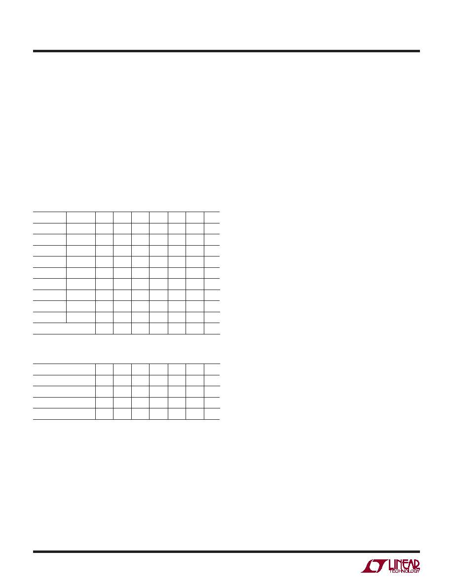
Table 1. Slave Address Map (LTC2631-Z)
CA1
CA0
A6
A5
A4
A3
A2
A1
A0
GND
0
1
0
GND
FLOAT
0
1
0
1
GND
VCC
0
100
1
0
FLOAT
GND
0
1
0
1
FLOAT
0
1
0
FLOAT
VCC
0
1
000
0
1
VCC
GND
0
1
0
1
0
VCC
FLOAT
0
1
0
1
VCC
0
1
100
0
GLOBAL ADDRESS
1
0
1
Table 2. Slave Address Map (LTC2631-M)
CA0
A6
A5
A4
A3
A2
A1
A0
GND
0
1
0
FLOAT
0
1
0
1
VCC
0
100
1
0
GLOBAL ADDRESS
1
0
1
In addition to the address selected by the address pins,
the part also responds to a global address. This address
allows a common write to all LTC2631 parts to be accom-
plished using one 3-byte write transaction on the I2C bus.
The global address, listed at the end of Tables 1 and 2, is
a 7-bit hardwired address not selectable by CA0/CA1. If
another address is required, please consult the factory.
The maximum capacitive load allowed on the CA0/CA1
address pins is 10pF, as these pins are driven during ad-
dress detection to determine if they are oating.
Write Word Protocol
The master initiates communication with the LTC2631 with
a START condition and a 7-bit slave address followed by the
Write bit (W) = 0. The LTC2631 acknowledges by pulling
the SDA pin low at the 9th clock if the 7-bit slave address
matches the address of the part (set by CA0/CA1) or the
global address. The master then transmits three bytes
of data. The LTC2631 acknowledges each byte of data
by pulling the SDA line low at the 9th clock of each data
byte transmission. After receiving three complete bytes
of data, the LTC2631 executes the command specied in
the 24-bit input word.
If more than three data bytes are transmitted after a valid
7-bit slave address, the LTC2631 does not acknowledge the
extra bytes of data (SDA is high during the 9th clock).
The format of the three data bytes is shown in Figure 3.
The rst byte of the input word consists of the 4-bit com-
mand, followed by four don’t care bits. The next two bytes
contain the 16-bit data word, which consists of the 12-,
10- or 8-bit input code, MSB to LSB, followed by 4, 6 or 8
don’t-care bits (LTC2631-12, LTC2631-10 and LTC2631-8
respectively). A typical LTC2631 write transaction is
shown in Figure 4.
The command bit assignments (C3-C0) are shown in
Table 3. The rst four commands in the table consist of
write and update operations. A write operation loads a
16-bit data word from the 32-bit shift register into the
input register. In an update operation, the data word is
copied from the input register to the DAC register and
converted to an analog voltage at the DAC output. The
update operation also powers up the DAC if it had been in
power-down mode. The data path and registers are shown
in the Block Diagram.
相关PDF资料 |
PDF描述 |
|---|---|
| LTC2631ITS8-LZ10#PBF | SERIAL INPUT LOADING, 3.8 us SETTLING TIME, 10-BIT DAC, PDSO8 |
| LTC2631ITS8-LZ12#PBF | SERIAL INPUT LOADING, 4.1 us SETTLING TIME, 12-BIT DAC, PDSO8 |
| LTC2631ITS8-LZ8#PBF | SERIAL INPUT LOADING, 3.2 us SETTLING TIME, 8-BIT DAC, PDSO8 |
| LTC2631ACTS8-HM12#TRPBF | SERIAL INPUT LOADING, 4.6 us SETTLING TIME, 12-BIT DAC, PDSO8 |
| LTC2631ACTS8-HZ12#TRPBF | SERIAL INPUT LOADING, 4.6 us SETTLING TIME, 12-BIT DAC, PDSO8 |
相关代理商/技术参数 |
参数描述 |
|---|---|
| LTC2631ITS8-LZ10#TRMPBF | 功能描述:IC DAC 10BIT VOUT TSOT23-8 RoHS:是 类别:集成电路 (IC) >> 数据采集 - 数模转换器 系列:- 产品培训模块:Lead (SnPb) Finish for COTS Obsolescence Mitigation Program 标准包装:58 系列:- 设置时间:6µs 位数:8 数据接口:并联 转换器数目:4 电压电源:双 ± 功率耗散(最大):640mW 工作温度:-40°C ~ 85°C 安装类型:表面贴装 封装/外壳:24-SSOP(0.209",5.30mm 宽) 供应商设备封装:24-SSOP 包装:管件 输出数目和类型:4 电压,单极;4 电压,双极 采样率(每秒):* |
| LTC2631ITS8-LZ10#TRPBF | 功能描述:IC DAC 10BIT I2C V-OUT TSOT23-8 RoHS:是 类别:集成电路 (IC) >> 数据采集 - 数模转换器 系列:- 产品培训模块:Data Converter Fundamentals DAC Architectures 设计资源:Unipolar, Precision DC Digital-to-Analog Conversion using AD5450/1/2/3 8-14-Bit DACs (CN0052) Precision, Bipolar, Configuration for AD5450/1/2/3 8-14bit Multiplying DACs (CN0053) AC Signal Processing Using AD5450/1/2/3 Current Output DACs (CN0054) Programmable Gain Element Using AD5450/1/2/3 Current Output DAC Family (CN0055) Single Supply Low Noise LED Current Source Driver Using a Current Output DAC in the Reverse Mode (CN0139) 标准包装:10,000 系列:- 设置时间:- 位数:12 数据接口:DSP,MICROWIRE?,QSPI?,串行,SPI? 转换器数目:1 电压电源:单电源 功率耗散(最大):- 工作温度:-40°C ~ 125°C 安装类型:表面贴装 封装/外壳:SOT-23-8 薄型,TSOT-23-8 供应商设备封装:TSOT-23-8 包装:带卷 (TR) 输出数目和类型:1 电流,单极;1 电流,双极 采样率(每秒):2.7M |
| LTC2631ITS8-LZ12#TRMPBF | 功能描述:IC DAC 12BIT VOUT TSOT23-8 RoHS:是 类别:集成电路 (IC) >> 数据采集 - 数模转换器 系列:- 产品培训模块:Lead (SnPb) Finish for COTS Obsolescence Mitigation Program 标准包装:58 系列:- 设置时间:6µs 位数:8 数据接口:并联 转换器数目:4 电压电源:双 ± 功率耗散(最大):640mW 工作温度:-40°C ~ 85°C 安装类型:表面贴装 封装/外壳:24-SSOP(0.209",5.30mm 宽) 供应商设备封装:24-SSOP 包装:管件 输出数目和类型:4 电压,单极;4 电压,双极 采样率(每秒):* |
| LTC2631ITS8-LZ12#TRPBF | 功能描述:IC DAC 12BIT VOUT TSOT23-8 RoHS:是 类别:集成电路 (IC) >> 数据采集 - 数模转换器 系列:- 产品培训模块:Data Converter Fundamentals DAC Architectures 设计资源:Unipolar, Precision DC Digital-to-Analog Conversion using AD5450/1/2/3 8-14-Bit DACs (CN0052) Precision, Bipolar, Configuration for AD5450/1/2/3 8-14bit Multiplying DACs (CN0053) AC Signal Processing Using AD5450/1/2/3 Current Output DACs (CN0054) Programmable Gain Element Using AD5450/1/2/3 Current Output DAC Family (CN0055) Single Supply Low Noise LED Current Source Driver Using a Current Output DAC in the Reverse Mode (CN0139) 标准包装:10,000 系列:- 设置时间:- 位数:12 数据接口:DSP,MICROWIRE?,QSPI?,串行,SPI? 转换器数目:1 电压电源:单电源 功率耗散(最大):- 工作温度:-40°C ~ 125°C 安装类型:表面贴装 封装/外壳:SOT-23-8 薄型,TSOT-23-8 供应商设备封装:TSOT-23-8 包装:带卷 (TR) 输出数目和类型:1 电流,单极;1 电流,双极 采样率(每秒):2.7M |
| LTC2631ITS8-LZ8#TRMPBF | 功能描述:IC DAC 8BIT VOUT TSOT23-8 RoHS:是 类别:集成电路 (IC) >> 数据采集 - 数模转换器 系列:- 产品培训模块:Data Converter Fundamentals DAC Architectures 设计资源:Unipolar, Precision DC Digital-to-Analog Conversion using AD5450/1/2/3 8-14-Bit DACs (CN0052) Precision, Bipolar, Configuration for AD5450/1/2/3 8-14bit Multiplying DACs (CN0053) AC Signal Processing Using AD5450/1/2/3 Current Output DACs (CN0054) Programmable Gain Element Using AD5450/1/2/3 Current Output DAC Family (CN0055) Single Supply Low Noise LED Current Source Driver Using a Current Output DAC in the Reverse Mode (CN0139) 标准包装:10,000 系列:- 设置时间:- 位数:12 数据接口:DSP,MICROWIRE?,QSPI?,串行,SPI? 转换器数目:1 电压电源:单电源 功率耗散(最大):- 工作温度:-40°C ~ 125°C 安装类型:表面贴装 封装/外壳:SOT-23-8 薄型,TSOT-23-8 供应商设备封装:TSOT-23-8 包装:带卷 (TR) 输出数目和类型:1 电流,单极;1 电流,双极 采样率(每秒):2.7M |
发布紧急采购,3分钟左右您将得到回复。