- 您现在的位置:买卖IC网 > PDF目录39421 > LTC2631ITS8-LM8#PBF (LINEAR TECHNOLOGY CORP) SERIAL INPUT LOADING, 3.2 us SETTLING TIME, 8-BIT DAC, PDSO8 PDF资料下载
参数资料
| 型号: | LTC2631ITS8-LM8#PBF |
| 厂商: | LINEAR TECHNOLOGY CORP |
| 元件分类: | DAC |
| 英文描述: | SERIAL INPUT LOADING, 3.2 us SETTLING TIME, 8-BIT DAC, PDSO8 |
| 封装: | LEAD FREE, PLASTIC, MO-193, TSOT-23, 8 PIN |
| 文件页数: | 16/28页 |
| 文件大小: | 349K |
| 代理商: | LTC2631ITS8-LM8#PBF |
第1页第2页第3页第4页第5页第6页第7页第8页第9页第10页第11页第12页第13页第14页第15页当前第16页第17页第18页第19页第20页第21页第22页第23页第24页第25页第26页第27页第28页
LTC2631
23
2631fa
OPERATION
Table 3. Command Codes
COMMAND*
C3
C2
C1
C0
0
Write to Input Register
0
1
Update (Power Up) DAC Register
0
1
Write to and Update (Power Up) DAC Register
0
1
0
Power Down
0
1
0
Select Internal Reference
0
1
Select External Reference
*Command codes not shown are reserved and should not be used.
Reference Modes
For applications where an accurate external reference is
not available, the LTC2631 has a user selectable, inte-
grated reference. The LTC2631-LM/LTC2631-LZ provide
a full-scale output of 2.5V. The LTC2631-HM/LTC2631-HZ
provide a full-scale output of 4.096V. The internal reference
can be useful in applications where the supply voltage is
poorly regulated. Internal Reference mode can be selected
by using command 0110, and is the power-on default for
LTC2631-HZ/LTC2631-LZ, as well as for LTC2631-HM/
LTC2631-LM when REF_SEL is tied high.
The 10ppm/°C, 1.25V (LTC2631-LM/LTC2631-LZ) or
2.048V (LTC2631-HM/LTC2631-HZ) internal reference
is available at the REF pin. Adding bypass capacitance
to the REF pin will improve noise performance; 0.33μF
is recommended, and up to 10μF can be driven without
oscillation. This output must be buffered when driving
external DC load current.
Alternatively, the DAC can operate in External Reference
mode using command 0111. In this mode, an input voltage
supplied externally to the REF pin provides the reference
(0V ≤ VREF ≤ VCC) and the supply current is reduced.
External Reference mode is the power-on default for
LTC2631-HM/LTC2631-LM when REF_SEL is tied low.
The reference mode of LTC2631-HZ/LTC2631-LZ can be
changed only by software command. The same is true for
LTC2631-HM/LTC2631-LM after power-on, after which the
logic state on REF_SEL is ignored.
Power-Down Mode
For power-constrained applications, the LTC2631’s power-
down mode can be used to reduce the supply current
whenever the DAC output is not needed. When in power-
down, the buffer amplier, bias circuit, and reference circuit
are disabled and draw essentially zero current. The DAC
output is put into a high-impedance state, and the output
pin is passively pulled to ground through a 200kΩ resistor.
Input and DAC register contents are not disturbed during
power-down.
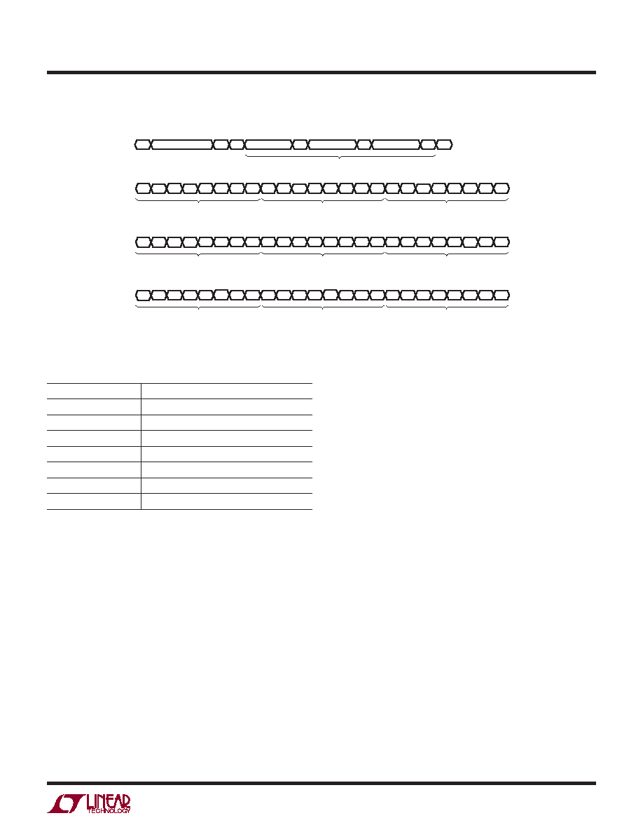
Figure 3. Command and Data Input Format
C3
1ST DATA BYTE
Input Word (LTC2631-12)
Write Word Protocol for LTC2631
C2
C1
C0
X
D9
D10
D11
S
WA
SLAVE ADDRESS
1ST DATA BYTE
D8
D7
D6
D5
D4
D3 D2
D1
D0
X
A
2ND DATA BYTE
A
3RD DATA BYTE
A
P
2631 F03
2ND DATA BYTE
INPUT WORD
3RD DATA BYTE
C3
1ST DATA BYTE
Input Word (LTC2631-10)
C2
C1
C0
X
D7
D8
D9
D6
D5
D4
D3
D2
D1 D0
XX
X
2ND DATA BYTE
3RD DATA BYTE
C3
1ST DATA BYTE
Input Word (LTC2631-8)
C2
C1
C0
X
D5
D6
D7
D4
D3
D2
D1
D0
X
XX
X
2ND DATA BYTE
3RD DATA BYTE
相关PDF资料 |
PDF描述 |
|---|---|
| LTC2631ITS8-LZ10#PBF | SERIAL INPUT LOADING, 3.8 us SETTLING TIME, 10-BIT DAC, PDSO8 |
| LTC2631ITS8-LZ12#PBF | SERIAL INPUT LOADING, 4.1 us SETTLING TIME, 12-BIT DAC, PDSO8 |
| LTC2631ITS8-LZ8#PBF | SERIAL INPUT LOADING, 3.2 us SETTLING TIME, 8-BIT DAC, PDSO8 |
| LTC2631ACTS8-HM12#TRPBF | SERIAL INPUT LOADING, 4.6 us SETTLING TIME, 12-BIT DAC, PDSO8 |
| LTC2631ACTS8-HZ12#TRPBF | SERIAL INPUT LOADING, 4.6 us SETTLING TIME, 12-BIT DAC, PDSO8 |
相关代理商/技术参数 |
参数描述 |
|---|---|
| LTC2631ITS8-LZ10#TRMPBF | 功能描述:IC DAC 10BIT VOUT TSOT23-8 RoHS:是 类别:集成电路 (IC) >> 数据采集 - 数模转换器 系列:- 产品培训模块:Lead (SnPb) Finish for COTS Obsolescence Mitigation Program 标准包装:58 系列:- 设置时间:6µs 位数:8 数据接口:并联 转换器数目:4 电压电源:双 ± 功率耗散(最大):640mW 工作温度:-40°C ~ 85°C 安装类型:表面贴装 封装/外壳:24-SSOP(0.209",5.30mm 宽) 供应商设备封装:24-SSOP 包装:管件 输出数目和类型:4 电压,单极;4 电压,双极 采样率(每秒):* |
| LTC2631ITS8-LZ10#TRPBF | 功能描述:IC DAC 10BIT I2C V-OUT TSOT23-8 RoHS:是 类别:集成电路 (IC) >> 数据采集 - 数模转换器 系列:- 产品培训模块:Data Converter Fundamentals DAC Architectures 设计资源:Unipolar, Precision DC Digital-to-Analog Conversion using AD5450/1/2/3 8-14-Bit DACs (CN0052) Precision, Bipolar, Configuration for AD5450/1/2/3 8-14bit Multiplying DACs (CN0053) AC Signal Processing Using AD5450/1/2/3 Current Output DACs (CN0054) Programmable Gain Element Using AD5450/1/2/3 Current Output DAC Family (CN0055) Single Supply Low Noise LED Current Source Driver Using a Current Output DAC in the Reverse Mode (CN0139) 标准包装:10,000 系列:- 设置时间:- 位数:12 数据接口:DSP,MICROWIRE?,QSPI?,串行,SPI? 转换器数目:1 电压电源:单电源 功率耗散(最大):- 工作温度:-40°C ~ 125°C 安装类型:表面贴装 封装/外壳:SOT-23-8 薄型,TSOT-23-8 供应商设备封装:TSOT-23-8 包装:带卷 (TR) 输出数目和类型:1 电流,单极;1 电流,双极 采样率(每秒):2.7M |
| LTC2631ITS8-LZ12#TRMPBF | 功能描述:IC DAC 12BIT VOUT TSOT23-8 RoHS:是 类别:集成电路 (IC) >> 数据采集 - 数模转换器 系列:- 产品培训模块:Lead (SnPb) Finish for COTS Obsolescence Mitigation Program 标准包装:58 系列:- 设置时间:6µs 位数:8 数据接口:并联 转换器数目:4 电压电源:双 ± 功率耗散(最大):640mW 工作温度:-40°C ~ 85°C 安装类型:表面贴装 封装/外壳:24-SSOP(0.209",5.30mm 宽) 供应商设备封装:24-SSOP 包装:管件 输出数目和类型:4 电压,单极;4 电压,双极 采样率(每秒):* |
| LTC2631ITS8-LZ12#TRPBF | 功能描述:IC DAC 12BIT VOUT TSOT23-8 RoHS:是 类别:集成电路 (IC) >> 数据采集 - 数模转换器 系列:- 产品培训模块:Data Converter Fundamentals DAC Architectures 设计资源:Unipolar, Precision DC Digital-to-Analog Conversion using AD5450/1/2/3 8-14-Bit DACs (CN0052) Precision, Bipolar, Configuration for AD5450/1/2/3 8-14bit Multiplying DACs (CN0053) AC Signal Processing Using AD5450/1/2/3 Current Output DACs (CN0054) Programmable Gain Element Using AD5450/1/2/3 Current Output DAC Family (CN0055) Single Supply Low Noise LED Current Source Driver Using a Current Output DAC in the Reverse Mode (CN0139) 标准包装:10,000 系列:- 设置时间:- 位数:12 数据接口:DSP,MICROWIRE?,QSPI?,串行,SPI? 转换器数目:1 电压电源:单电源 功率耗散(最大):- 工作温度:-40°C ~ 125°C 安装类型:表面贴装 封装/外壳:SOT-23-8 薄型,TSOT-23-8 供应商设备封装:TSOT-23-8 包装:带卷 (TR) 输出数目和类型:1 电流,单极;1 电流,双极 采样率(每秒):2.7M |
| LTC2631ITS8-LZ8#TRMPBF | 功能描述:IC DAC 8BIT VOUT TSOT23-8 RoHS:是 类别:集成电路 (IC) >> 数据采集 - 数模转换器 系列:- 产品培训模块:Data Converter Fundamentals DAC Architectures 设计资源:Unipolar, Precision DC Digital-to-Analog Conversion using AD5450/1/2/3 8-14-Bit DACs (CN0052) Precision, Bipolar, Configuration for AD5450/1/2/3 8-14bit Multiplying DACs (CN0053) AC Signal Processing Using AD5450/1/2/3 Current Output DACs (CN0054) Programmable Gain Element Using AD5450/1/2/3 Current Output DAC Family (CN0055) Single Supply Low Noise LED Current Source Driver Using a Current Output DAC in the Reverse Mode (CN0139) 标准包装:10,000 系列:- 设置时间:- 位数:12 数据接口:DSP,MICROWIRE?,QSPI?,串行,SPI? 转换器数目:1 电压电源:单电源 功率耗散(最大):- 工作温度:-40°C ~ 125°C 安装类型:表面贴装 封装/外壳:SOT-23-8 薄型,TSOT-23-8 供应商设备封装:TSOT-23-8 包装:带卷 (TR) 输出数目和类型:1 电流,单极;1 电流,双极 采样率(每秒):2.7M |
发布紧急采购,3分钟左右您将得到回复。