- 您现在的位置:买卖IC网 > PDF目录39424 > LTC263ACSC6-LZ12#TRPBF (LINEAR TECHNOLOGY CORP) SERIAL INPUT LOADING, 4.4 us SETTLING TIME, 12-BIT DAC, PDSO6 PDF资料下载
参数资料
| 型号: | LTC263ACSC6-LZ12#TRPBF |
| 厂商: | LINEAR TECHNOLOGY CORP |
| 元件分类: | DAC |
| 英文描述: | SERIAL INPUT LOADING, 4.4 us SETTLING TIME, 12-BIT DAC, PDSO6 |
| 封装: | LEAD FREE, PLASTIC, MO-203AB, SC-70, 6 PIN |
| 文件页数: | 6/20页 |
| 文件大小: | 341K |
| 代理商: | LTC263ACSC6-LZ12#TRPBF |
LTC2630
14
2630f
Serial Interface
The
CS/LD input is level triggered. When this input is taken
low, it acts as a chip-select signal, enabling the SDI and
SCK buffers and the input shift register. Data (SDI input)
is transferred at the next 24 rising SCK edges. The 4-bit
command, C3-C0, is loaded rst; then 4 don’t-care bits;
and nally the 16-bit data word. The data word comprises
the 12-, 10- or 8-bit input code, ordered MSB-to-LSB, fol-
lowed by 4, 6 or 8 don’t-care bits (LTC2630-12, -10 and
-8 respectively; see Figure 2). Data can only be transferred
to the device when the
CS/LD signal is low, beginning on
the rst rising edge of SCK. SCK may be high or low at
the falling edge of
CS/LD. The rising edge of CS/LD ends
the data transfer and causes the device to execute the
command specied in the 24-bit input sequence. The
complete sequence is shown in Figure 3a.
The command (C3-C0) assignments are shown in Table 1.
The rst three commands in the table consist of write and
update operations. A Write operation loads a 16-bit data
word from the 24-bit shift register into the input register.
In an Update operation, the input register is copied to the
DAC register and converted to an analog voltage at the
DAC output. Write to and Update combines the rst two
commands. The Update operation also powers up the
DAC if it had been in power-down mode. The data path
and registers are shown in the Block Diagram.
OPERATION
While the minimum input sequence is 24 bits, it may
optionally be extended to 32 bits to accommodate micro-
processors that have a minimum word width of 16 bits
(2 bytes). To use the 32-bit width, 8 don’t-care bits are trans-
ferred to the device rst, followed by the 24-bit sequence
described. Figure 3b shows the 32-bit sequence.
The 16-bit data word is ignored for all commands that do
not include a Write operation.
Power-Down Mode
For power-constrained applications, power-down mode
can be used to reduce the supply current whenever the
DAC output is not needed. When in power-down, the buffer
amplier, bias circuit, and reference circuit are disabled and
draw essentially zero current. The DAC output is put into
a high-impedance state, and the output pin is passively
pulled to ground through a 200k
Ω resistor. Input and DAC
register contents are not disturbed during power-down.
The DAC can be put into power-down mode by using
command 0100. The supply current is reduced to 1.5A
maximum when the DAC is powered down.
Normal operation resumes after executing any command
that includes a DAC update, as shown in Table 1. The DAC
is powered up and its voltage output is updated. Normal
settling is delayed while the bias, reference, and amplier
circuits are re-enabled. The power up delay time is 18
μs
for settling to 12 bits.
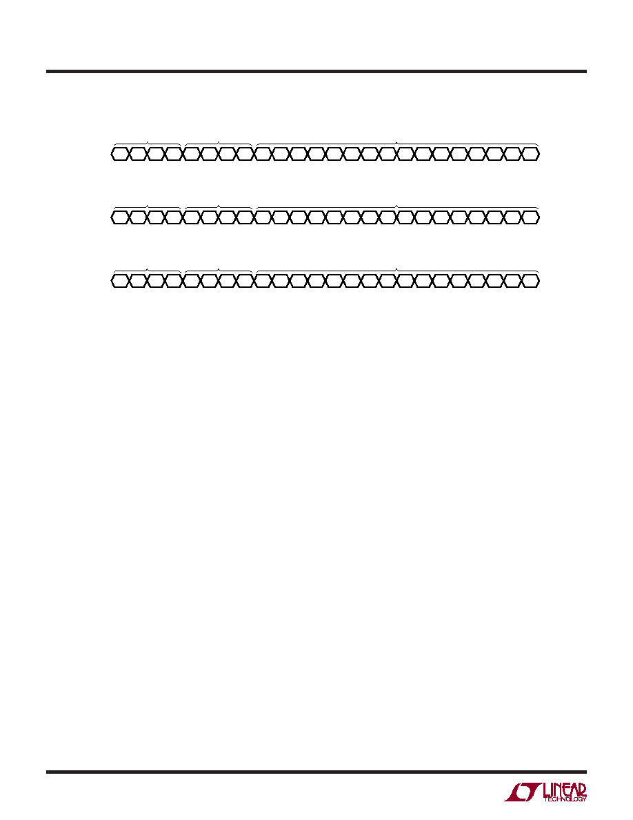
2630 F02
C3
COMMAND
4 DON'T-CARE BITS
MSB
LSB
DATA (12 BITS + 4 DON'T-CARE BITS)
C2
C1
C0
X
D11 D10
D9
D8
D7
D6
D5
D4
D3
D2
D1
D0
X
C3
COMMAND
4 DON'T-CARE BITS
DATA (10 BITS + 6 DON'T-CARE BITS)
C2
C1
C0
X
D9
D8
D7
D6
D5
D4
D3
D2
D1
D0
X
C3
COMMAND
INPUT WORD (LTC2630-12)
INPUT WORD (LTC2630-10)
INPUT WORD (LTC2630-8)
4 DON'T-CARE BITS
DATA (8 BITS + 8 DON'T-CARE BITS)
C2
C1
C0
X
D7
D6
D5
D4
D3
D2
D1
D0
X
Figure 2. Command and Data Input Format
相关PDF资料 |
PDF描述 |
|---|---|
| LTC2641IS8-16#PBF | 16-BIT DAC, PDSO8 |
| LTC2641IS8-16#TRPBF | 16-BIT DAC, PDSO8 |
| LTC2641CS8-16#PBF | 16-BIT DAC, PDSO8 |
| LTC2641CS8-16#TRPBF | 16-BIT DAC, PDSO8 |
| LTC2752AILX#PBF | 16-BIT DAC, PQFP48 |
相关代理商/技术参数 |
参数描述 |
|---|---|
| LTC2640ACTS8-HM12#PBF | 制造商:Linear Technology 功能描述:SINGLE 12/10/8-BIT SPI VOUT DACS WITH 10PPM/DEGREE C REFERENCE |
| LTC2640ACTS8-HM12#TRMPBF | 功能描述:IC DAC 12BIT VOUT W/REF TSOT23-8 RoHS:是 类别:集成电路 (IC) >> 数据采集 - 数模转换器 系列:- 产品培训模块:Lead (SnPb) Finish for COTS Obsolescence Mitigation Program 标准包装:58 系列:- 设置时间:6µs 位数:8 数据接口:并联 转换器数目:4 电压电源:双 ± 功率耗散(最大):640mW 工作温度:-40°C ~ 85°C 安装类型:表面贴装 封装/外壳:24-SSOP(0.209",5.30mm 宽) 供应商设备封装:24-SSOP 包装:管件 输出数目和类型:4 电压,单极;4 电压,双极 采样率(每秒):* |
| LTC2640ACTS8-HM12#TRPBF | 功能描述:IC DAC 12BIT VOUT W/REF TSOT23-8 RoHS:是 类别:集成电路 (IC) >> 数据采集 - 数模转换器 系列:- 产品培训模块:Lead (SnPb) Finish for COTS Obsolescence Mitigation Program 标准包装:58 系列:- 设置时间:6µs 位数:8 数据接口:并联 转换器数目:4 电压电源:双 ± 功率耗散(最大):640mW 工作温度:-40°C ~ 85°C 安装类型:表面贴装 封装/外壳:24-SSOP(0.209",5.30mm 宽) 供应商设备封装:24-SSOP 包装:管件 输出数目和类型:4 电压,单极;4 电压,双极 采样率(每秒):* |
| LTC2640ACTS8-HZ12#PBF | 制造商:Linear Technology 功能描述:SINGLE 12/10/8-BIT SPI VOUT DACS WITH 10PPM/DEGREE C REFERENCE |
| LTC2640ACTS8-HZ12#TRMPBF | 功能描述:IC DAC 12BIT VOUT W/REF TSOT23-8 RoHS:是 类别:集成电路 (IC) >> 数据采集 - 数模转换器 系列:- 产品培训模块:Lead (SnPb) Finish for COTS Obsolescence Mitigation Program 标准包装:58 系列:- 设置时间:6µs 位数:8 数据接口:并联 转换器数目:4 电压电源:双 ± 功率耗散(最大):640mW 工作温度:-40°C ~ 85°C 安装类型:表面贴装 封装/外壳:24-SSOP(0.209",5.30mm 宽) 供应商设备封装:24-SSOP 包装:管件 输出数目和类型:4 电压,单极;4 电压,双极 采样率(每秒):* |
发布紧急采购,3分钟左右您将得到回复。