- 您现在的位置:买卖IC网 > PDF目录2006 > LTC2752ACLX#PBF (Linear Technology)IC DAC 16BIT DUAL CUR OUT 48LQFP PDF资料下载
参数资料
| 型号: | LTC2752ACLX#PBF |
| 厂商: | Linear Technology |
| 文件页数: | 5/24页 |
| 文件大小: | 0K |
| 描述: | IC DAC 16BIT DUAL CUR OUT 48LQFP |
| 标准包装: | 250 |
| 系列: | SoftSpan™ |
| 设置时间: | 2µs |
| 位数: | 16 |
| 数据接口: | 串行,SPI? |
| 转换器数目: | 2 |
| 电压电源: | 单电源 |
| 工作温度: | 0°C ~ 70°C |
| 安装类型: | 表面贴装 |
| 封装/外壳: | 48-LQFP |
| 供应商设备封装: | 48-LQFP(7x7) |
| 包装: | 托盘 |
| 输出数目和类型: | 2 电流,单极;2 电流,双极 |
| 采样率(每秒): | * |
| 配用: | DC1684A-B-ND - BOARD DAC LTC2752 |
LTC2752
2752f
Output Ranges
TheLTC2752isadual,current-output,serial-inputprecision
multiplying DAC with selectable output ranges. Ranges
can either be programmed in software for maximum flex-
ibility—each of the DACs can be programmed to any one
ofsixoutputranges—orhardwiredthroughpin-strapping.
Two unipolar ranges are available (0V to 5V and 0V to 10V),
and four bipolar ranges (±2.5V, ±5V, ±10V and –2.5V to
7.5V). These ranges are obtained when an external pre-
cision 5V reference is used. The output ranges for other
reference voltages are easy to calculate by observing that
each range is a multiple of the external reference voltage.
Therangescanthenbeexpressed:0 to 1
×,0 to 2×,±0.5×,
±1
×, ±2×, and –0.5× to 1.5×.
Manual Span Configuration
Multiple output ranges are not needed in some applica-
tions. To configure the LTC2752 to operate in a single span
without additional operational overhead, tie the M-SPAN
pin directly to VDD. The active output range for all DACs is
then set via hardware pin strapping of pins S2, S1 and S0
(rather than through the SPI port); and Write and Update
commands have no effect on the active output span. See
Figure 1 and Table 3.
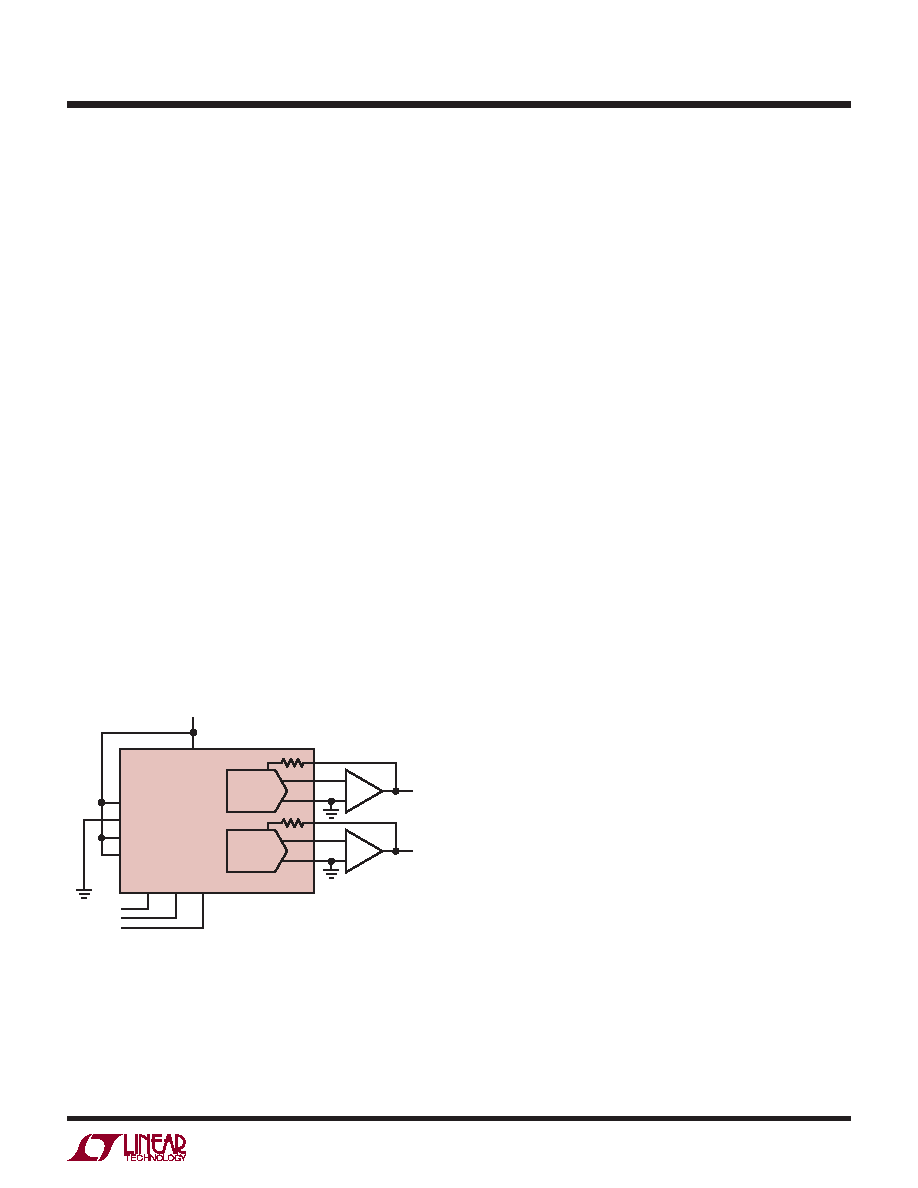
Figure 1. Using M-SPAN to Configure the LTC2752
for Single-Span Operation (±10V Range Shown)
LTC2752
M-SPAN
S2
S1
S0
2752 F01
CS/LD SDI SCK
VDD
DAC A
±10V
DAC B
–
+
–
+
operaTion
Tie the M-SPAN pin to ground for normal SoftSpan
operation.
Input and DAC Registers
The LTC2752 has 5 internal registers for each DAC, a total
of 10 registers (see Block Diagram). Each DAC channel
has two sets of double-buffered registers—one set for the
code data, and one for the output range of the DAC—plus
one readback register. Double buffering provides the ca-
pability to simultaneously update the span (output range)
and code, which allows smooth voltage transitions when
changing output ranges. It also permits the simultaneous
updating of multiple DACs.
Each set of double-buffered registers comprises an Input
register and a DAC register.
Input register: The Write operation shifts data from the
SDI pin into a chosen Input register. The Input registers
are holding buffers; Write operations do not affect the
DAC outputs.
DAC register: The Update operation copies the contents
of an Input register to its associated DAC register. The
contents of a DAC register directly updates the associated
DAC output voltage or output range.
Note that updates always include both Code and Span
register sets; but the values held in the DAC registers will
only change if the associated Input register values have
previously been changed via a Write operation.
Serial Interface
When the CS/LD pin is taken low, the data on the SDI
pin is loaded into the shift register on the rising edge of
the clock (SCK pin). The minimum (24-bit wide) loading
sequence required for the LTC2752 is a 4-bit command
word (C3 C2 C1 C0), followed by a 4-bit address word
(A3 A2 A1 A0) and 16 data (span or code) bits, MSB first.
Figure 2 shows the SDI input word syntax to use when
相关PDF资料 |
PDF描述 |
|---|---|
| LTC2753AIUK-16#TRPBF | IC DAC 16BIT DUAL 48-QFN |
| LTC2754AIUKG-16#PBF | IC DAC 16BIT QUAD IOUT 52-QFN |
| LTC2755AIUP-16#PBF | IC DAC 16BIT CUR OUT 64-QFN |
| LTC2757ACLX#PBF | IC DAC 18BIT PAR 48LQFP |
| LTC2758AILX#PBF | IC DAC 18BIT SPI/SRL 48-LQFP |
相关代理商/技术参数 |
参数描述 |
|---|---|
| LTC2752AILX#PBF | 功能描述:IC DAC 16BIT DUAL CUR OUT 48LQFP RoHS:是 类别:集成电路 (IC) >> 数据采集 - 数模转换器 系列:SoftSpan™ 产品培训模块:Data Converter Fundamentals DAC Architectures 标准包装:750 系列:- 设置时间:7µs 位数:16 数据接口:并联 转换器数目:1 电压电源:双 ± 功率耗散(最大):100mW 工作温度:0°C ~ 70°C 安装类型:表面贴装 封装/外壳:28-LCC(J 形引线) 供应商设备封装:28-PLCC(11.51x11.51) 包装:带卷 (TR) 输出数目和类型:1 电压,单极;1 电压,双极 采样率(每秒):143k |
| LTC2752BCLX#PBF | 功能描述:IC DAC 16BIT DUAL CUR OUT 48LQFP RoHS:是 类别:集成电路 (IC) >> 数据采集 - 数模转换器 系列:SoftSpan™ 产品培训模块:Lead (SnPb) Finish for COTS Obsolescence Mitigation Program 标准包装:50 系列:- 设置时间:4µs 位数:12 数据接口:串行 转换器数目:2 电压电源:单电源 功率耗散(最大):- 工作温度:-40°C ~ 85°C 安装类型:表面贴装 封装/外壳:8-TSSOP,8-MSOP(0.118",3.00mm 宽) 供应商设备封装:8-uMAX 包装:管件 输出数目和类型:2 电压,单极 采样率(每秒):* 产品目录页面:1398 (CN2011-ZH PDF) |
| LTC2752BILX#PBF | 功能描述:IC DAC 16BIT DUAL CUR OUT 48LQFP RoHS:是 类别:集成电路 (IC) >> 数据采集 - 数模转换器 系列:SoftSpan™ 产品培训模块:Data Converter Fundamentals DAC Architectures 标准包装:750 系列:- 设置时间:7µs 位数:16 数据接口:并联 转换器数目:1 电压电源:双 ± 功率耗散(最大):100mW 工作温度:0°C ~ 70°C 安装类型:表面贴装 封装/外壳:28-LCC(J 形引线) 供应商设备封装:28-PLCC(11.51x11.51) 包装:带卷 (TR) 输出数目和类型:1 电压,单极;1 电压,双极 采样率(每秒):143k |
| LTC2753ACUK-16#PBF | 功能描述:IC DAC 16BIT DUAL 48-QFN RoHS:是 类别:集成电路 (IC) >> 数据采集 - 数模转换器 系列:SoftSpan™ 产品培训模块:Data Converter Fundamentals DAC Architectures 标准包装:750 系列:- 设置时间:7µs 位数:16 数据接口:并联 转换器数目:1 电压电源:双 ± 功率耗散(最大):100mW 工作温度:0°C ~ 70°C 安装类型:表面贴装 封装/外壳:28-LCC(J 形引线) 供应商设备封装:28-PLCC(11.51x11.51) 包装:带卷 (TR) 输出数目和类型:1 电压,单极;1 电压,双极 采样率(每秒):143k |
| LTC2753ACUK-16#TRPBF | 功能描述:IC DAC 16BIT DUAL 48-QFN RoHS:是 类别:集成电路 (IC) >> 数据采集 - 数模转换器 系列:SoftSpan™ 产品培训模块:Data Converter Fundamentals DAC Architectures 标准包装:750 系列:- 设置时间:7µs 位数:16 数据接口:并联 转换器数目:1 电压电源:双 ± 功率耗散(最大):100mW 工作温度:0°C ~ 70°C 安装类型:表面贴装 封装/外壳:28-LCC(J 形引线) 供应商设备封装:28-PLCC(11.51x11.51) 包装:带卷 (TR) 输出数目和类型:1 电压,单极;1 电压,双极 采样率(每秒):143k |
发布紧急采购,3分钟左右您将得到回复。