- 您现在的位置:买卖IC网 > PDF目录39424 > LTC2752AILX#PBF (LINEAR TECHNOLOGY CORP) 16-BIT DAC, PQFP48 PDF资料下载
参数资料
| 型号: | LTC2752AILX#PBF |
| 厂商: | LINEAR TECHNOLOGY CORP |
| 元件分类: | DAC |
| 英文描述: | 16-BIT DAC, PQFP48 |
| 封装: | 7 X 7 MM, LEAD FREE, PLASTIC, MS-026, LQFP-48 |
| 文件页数: | 14/24页 |
| 文件大小: | 360K |
| 代理商: | LTC2752AILX#PBF |
LTC2752
2752f
applicaTions inForMaTion
Op amp offset will contribute mostly to output offset and
gain error, and has minimal effect on INL and DNL. For
example,fortheLTC2752witha5Vreferencein5Vunipolar
mode, a 250V op amp offset will cause a 3.3LSB zero-
scale error and a 3.3LSB gain error; but only 0.75LSB of
INL degradation and 0.2LSB of DNL degradation.
While not directly addressed by the simple equations in
Tables 4 and 5, temperature effects can be handled just
as easily for unipolar and bipolar applications. First, con-
sult an op amp’s data sheet to find the worst-case VOS
and IB over temperature. Then, plug these numbers into
the VOS and IB equations from Table 5 and calculate the
temperature-induced effects.
For applications where fast settling time is important, Ap-
plicationNote74,ComponentandMeasurementAdvances
Ensure16-BitDACSettlingTime,offersathoroughdiscus-
sion of 16-bit DAC settling time and op amp selection.
Precision Voltage Reference Considerations
Much in the same way selecting an operational amplifier
for use with the LTC2752 is critical to the performance of
the system, selecting a precision voltage reference also
requires due diligence. The output voltage of the LTC2752
is directly affected by the voltage reference; thus, any
voltage reference error will appear as a DAC output volt-
age error.
There are three primary error sources to consider
when selecting a precision voltage reference for 16-bit
applications:outputvoltageinitialtolerance,outputvoltage
temperature coefficient and output voltage noise.
Initial reference output voltage tolerance, if uncorrected,
generates a full-scale error term. Choosing a reference
with low output voltage initial tolerance, like the LT1236
(±0.05%),minimizesthegainerrorcausedbythereference;
however, a calibration sequence that corrects for system
zero- and full-scale error is always recommended.
A reference’s output voltage temperature coefficient af-
fects not only the full-scale error, but can also affect the
circuit’s apparent INL and DNL performance. If a refer-
ence is chosen with a loose output voltage temperature
coefficient, then the DAC output voltage along its transfer
characteristicwillbeverydependentonambientconditions.
Minimizing the error due to reference temperature coef-
ficient can be achieved by choosing a precision reference
with a low output voltage temperature coefficient and/or
tightly controlling the ambient temperature of the circuit
to minimize temperature gradients.
As precision DAC applications move to 16-bit and higher
performance, reference output voltage noise may contrib-
ute a dominant share of the system’s noise floor. This in
turncandegradesystemdynamicrangeandsignal-to-noise
ratio. Care should be exercised in selecting a voltage refer-
encewithaslowanoutputnoisevoltageaspracticalforthe
system resolution desired. Precision voltage references,
like the LT1236 and LTC6655, produce low output noise in
the 0.1Hz to 10Hz region, well below the 16-bit LSB level
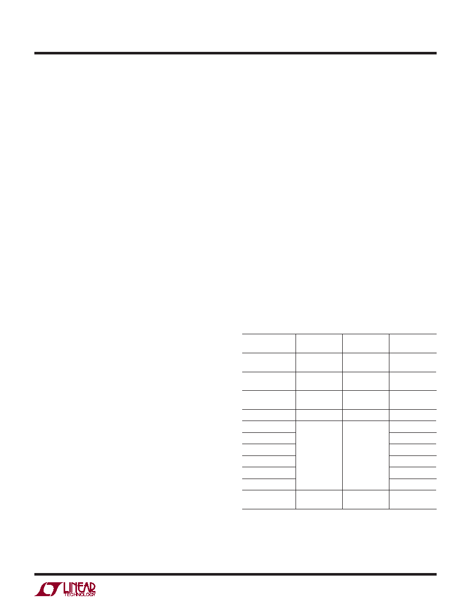
Table 7. Partial List of LTC Precision References Recommended
for Use with the LTC2752 with Relevant Specifications
REFERENCE
INITIAL
TOLERANCE
TEMPERATURE
DRIFT
0.1Hz to 10Hz
NOISE
LT1019A-5,
LT1019A-10
±0.05% Max
5ppm/°C Max
12VP-P
LT1236A-5,
LT1236A-10
±0.05% Max
5ppm/°C Max
3VP-P
LT1460A-5,
LT1460A-10
±0.075% Max
10ppm/°C Max
20VP-P
LT1790A-2.5
±0.05% Max
10ppm/°C Max
12VP-P
LTC6652A-2.048
±0.05% Max
5ppm/°C Max
2.1ppmP-P
LTC6652A-2.5
2.1ppmP-P
LTC6652A-3
2.1ppmP-P
LTC6652A-3.3
2.2ppmP-P
LTC6652A-4.096
2.3ppmP-P
LTC6652A-5
2.8ppmP-P
LT6655A-25,
LT6655A-5
±0.025% Max
2ppm/°C Max
0.25ppmP-P
相关PDF资料 |
PDF描述 |
|---|---|
| LTC2752ACLX#PBF | 16-BIT DAC, PQFP48 |
| LTC2752BCLX#PBF | 16-BIT DAC, PQFP48 |
| LTC2752BILX#PBF | 16-BIT DAC, PQFP48 |
| LTC2757ACLX#PBF | PARALLEL, WORD INPUT LOADING, 2.1 us SETTLING TIME, 18-BIT DAC, PQFP48 |
| LTC2757AILX#PBF | PARALLEL, WORD INPUT LOADING, 2.1 us SETTLING TIME, 18-BIT DAC, PQFP48 |
相关代理商/技术参数 |
参数描述 |
|---|---|
| LTC2752BCLX#PBF | 功能描述:IC DAC 16BIT DUAL CUR OUT 48LQFP RoHS:是 类别:集成电路 (IC) >> 数据采集 - 数模转换器 系列:SoftSpan™ 产品培训模块:Lead (SnPb) Finish for COTS Obsolescence Mitigation Program 标准包装:50 系列:- 设置时间:4µs 位数:12 数据接口:串行 转换器数目:2 电压电源:单电源 功率耗散(最大):- 工作温度:-40°C ~ 85°C 安装类型:表面贴装 封装/外壳:8-TSSOP,8-MSOP(0.118",3.00mm 宽) 供应商设备封装:8-uMAX 包装:管件 输出数目和类型:2 电压,单极 采样率(每秒):* 产品目录页面:1398 (CN2011-ZH PDF) |
| LTC2752BILX#PBF | 功能描述:IC DAC 16BIT DUAL CUR OUT 48LQFP RoHS:是 类别:集成电路 (IC) >> 数据采集 - 数模转换器 系列:SoftSpan™ 产品培训模块:Data Converter Fundamentals DAC Architectures 标准包装:750 系列:- 设置时间:7µs 位数:16 数据接口:并联 转换器数目:1 电压电源:双 ± 功率耗散(最大):100mW 工作温度:0°C ~ 70°C 安装类型:表面贴装 封装/外壳:28-LCC(J 形引线) 供应商设备封装:28-PLCC(11.51x11.51) 包装:带卷 (TR) 输出数目和类型:1 电压,单极;1 电压,双极 采样率(每秒):143k |
| LTC2753ACUK-16#PBF | 功能描述:IC DAC 16BIT DUAL 48-QFN RoHS:是 类别:集成电路 (IC) >> 数据采集 - 数模转换器 系列:SoftSpan™ 产品培训模块:Data Converter Fundamentals DAC Architectures 标准包装:750 系列:- 设置时间:7µs 位数:16 数据接口:并联 转换器数目:1 电压电源:双 ± 功率耗散(最大):100mW 工作温度:0°C ~ 70°C 安装类型:表面贴装 封装/外壳:28-LCC(J 形引线) 供应商设备封装:28-PLCC(11.51x11.51) 包装:带卷 (TR) 输出数目和类型:1 电压,单极;1 电压,双极 采样率(每秒):143k |
| LTC2753ACUK-16#TRPBF | 功能描述:IC DAC 16BIT DUAL 48-QFN RoHS:是 类别:集成电路 (IC) >> 数据采集 - 数模转换器 系列:SoftSpan™ 产品培训模块:Data Converter Fundamentals DAC Architectures 标准包装:750 系列:- 设置时间:7µs 位数:16 数据接口:并联 转换器数目:1 电压电源:双 ± 功率耗散(最大):100mW 工作温度:0°C ~ 70°C 安装类型:表面贴装 封装/外壳:28-LCC(J 形引线) 供应商设备封装:28-PLCC(11.51x11.51) 包装:带卷 (TR) 输出数目和类型:1 电压,单极;1 电压,双极 采样率(每秒):143k |
| LTC2753AIUK-16#PBF | 功能描述:IC DAC 16BIT DUAL 48-QFN RoHS:是 类别:集成电路 (IC) >> 数据采集 - 数模转换器 系列:SoftSpan™ 产品培训模块:Data Converter Fundamentals DAC Architectures 标准包装:750 系列:- 设置时间:7µs 位数:16 数据接口:并联 转换器数目:1 电压电源:双 ± 功率耗散(最大):100mW 工作温度:0°C ~ 70°C 安装类型:表面贴装 封装/外壳:28-LCC(J 形引线) 供应商设备封装:28-PLCC(11.51x11.51) 包装:带卷 (TR) 输出数目和类型:1 电压,单极;1 电压,双极 采样率(每秒):143k |
发布紧急采购,3分钟左右您将得到回复。