- 您现在的位置:买卖IC网 > PDF目录14057 > LTC3103EDD#PBF (Linear Technology)IC REG BUCK SYNC ADJ 0.3A 10DFN PDF资料下载
参数资料
| 型号: | LTC3103EDD#PBF |
| 厂商: | Linear Technology |
| 文件页数: | 13/20页 |
| 文件大小: | 0K |
| 描述: | IC REG BUCK SYNC ADJ 0.3A 10DFN |
| 标准包装: | 121 |
| 类型: | 降压(降压) |
| 输出类型: | 可调式 |
| 输出数: | 1 |
| 输出电压: | 0.6 V ~ 13.8 V |
| 输入电压: | 2.5 V ~ 15 V |
| PWM 型: | 电流模式,混合 |
| 频率 - 开关: | 1.2MHz |
| 电流 - 输出: | 300mA |
| 同步整流器: | 是 |
| 工作温度: | -40°C ~ 125°C |
| 安装类型: | 表面贴装 |
| 封装/外壳: | 10-WFDFN 裸露焊盘 |
| 包装: | 管件 |
| 供应商设备封装: | 10-DFN(3x3) |
�� �
�
�LTC3103�
�APPLICATIONS� INFORMATION�
�V� OUT� =� 0.6V� ?� ?� 1� +�
�f� ZERO� =�
�V� IN(MIN)� =�
�(�
�)�
�InputCapacitorSelection�
�The� V� IN� pin� provides� current� to� the� power� stages� of� the�
�buck� converter.� It� is� recommended� that� a� low� ESR� ceramic�
�capacitor� with� a� value� of� at� least� 10μF� be� used� to� bypass�
�the� pin.� These� capacitors� should� be� placed� as� close� to�
�the� pin� as� possible� and� should� have� a� short� return� path�
�to� the� GND� pin.�
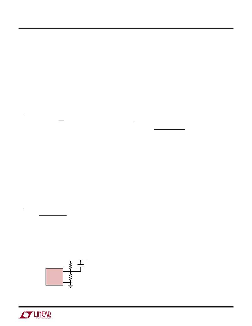
�Output� Voltage� Programming�
�The� output� voltage� is� set� by� a� resistive� divider� according�
�to� the� following� formula:�
�?� R2� ?�
�?�
�?� R1� ?�
�The� external� divider� is� connected� to� the� output� as� shown�
�in� Figure� 1.� Note� that� FB� divider� current� is� not� included� in�
�the� LTC3103� quiescent� current� specification.� For� improved�
�transient� response,� a� feedforward� capacitor,� C� FF� ,� may� be�
�placed� in� parallel� with� resistor� R2.� The� capacitor� modifies�
�the� loop� dynamics� by� adding� a� pole-zero� pair� to� the� loop�
�dynamics� which� generates� a� phase� boost� that� can� improve�
�the� phase� margin� and� increase� the� speed� of� the� transient�
�response,� resulting� in� smaller� voltage� deviation� on� load�
�transients.� The� zero� frequency� depends� not� only� on� the�
�value� of� the� feed� forward� capacitor,� but� also� on� the� upper�
�resistor� divider� resistor.� Specifically,� the� zero� frequency,�
�f� ZERO� ,� is� given� by� the� following� equation:�
�1�
�2� ?� π� ?� R2� ?� C� FF1�
�For� R2� resistor� values� of� ~1M� a� 12pF� ceramic� capacitor�
�will� suffice,� however� that� value� may� be� increased� or� de-�
�creased� to� optimize� the� converter’s� response� for� a� given�
�set� of� application� parameters.�
�V� OUT�
�R2� C� FF�
�FB�
�LTC3103� R1�
�GND�
�3103� F01�
�Figure� 1.� Setting� the� Output� Voltage�
�Minimum� Off-Time/On-Time� Considerations�
�The� maximum� duty� cycle� is� limited� in� the� LTC3103� by� the�
�boost� capacitor� refresh� time,� the� rise/fall� times� of� the� switch�
�as� well� as� propagation� delays� in� the� PWM� comparator,� the�
�level� shifts� and� the� gate� drive.� This� minimum� off� time� is�
�typically� 65ns� which� imposes� a� maximum� duty� cycle� of:�
�DC� MAX� =� 1� –� (f� ?� t� OFF(MIN)� )�
�where� f� is� the� 1.2MHz� switching� frequency� and� t� OFF(MIN)�
�is� the� minimum� off-time.� If� the� maximum� duty� cycle� is�
�surpassed,� due� to� a� dropping� input� voltage� for� example,�
�the� output� will� drop� out� of� regulation.� The� minimum� input�
�voltage� to� avoid� this� dropout� condition� is:�
�V� OUT�
�1–� f� ?� t� OFF(MIN)�
�Conversely,� the� minimum� on-time� is� the� smallest� duration�
�of� time� in� which� the� buck� switch� can� be� in� its� “on”� state.�
�This� time� is� limited� by� similar� factors� and� is� typically� 70ns.�
�In� forced� continuous� operation,� the� minimum� on-time� limit�
�imposes� a� minimum� duty� cycle� of:�
�DC� MIN� =� f� ?� t� ON(MIN)�
�where� t� ON(MIN)� is� the� minimum� on-time.� In� extreme� step-�
�down� ratios� where� the� minimum� duty� cycle� is� surpassed,�
�the� output� voltage� will� still� be� in� regulation� but� the� rectifier�
�switch� will� remain� on� for� more� than� one� cycle� and� sub-�
�harmonic� switching� will� occur� to� provide� a� higher� effective�
�duty� cycle.� The� result� is� higher� output� voltage� ripple.� This� is�
�an� acceptable� result� in� many� applications� so� this� constraint�
�may� not� be� of� critical� importance� in� some� cases.�
�Precise� Undervoltage� Lockout�
�The� LTC3103� is� in� shutdown� when� the� RUN� pin� is� low� and�
�active� when� the� pin� is� higher� than� the� RUN� pin� threshold.�
�The� rising� threshold� of� the� RUN� pin� comparator� is� an�
�accurate� 0.8V,� with� 60mV� of� hysteresis.� This� threshold� is�
�enabled� when� V� IN� is� above� the� 2.5V� minimum� value.� If� V� IN�
�is� lower� than� 2.5V,� an� internal� undervoltage� monitor� puts�
�the� part� in� shutdown� independent� of� the� RUN� pin� state.�
�The� RUN� pin� can� be� configured� as� a� precise� undervoltage�
�lockout� (UVLO)� on� the� V� IN� supply� with� a� resistive� divider�
�3103f�
�13�
�相关PDF资料 |
PDF描述 |
|---|---|
| VI-J6W-EZ | CONVERTER MOD DC/DC 5.5V 25W |
| ABC17DRES-S13 | CONN EDGECARD 34POS .100 EYELET |
| V24B12C150BG2 | CONVERTER MOD DC/DC 12V 150W |
| ASC15DREF-S13 | CONN EDGECARD 30POS .100 EXTEND |
| AMC15DREF-S13 | CONN EDGECARD 30POS .100 EXTEND |
相关代理商/技术参数 |
参数描述 |
|---|---|
| LTC3103EMSE#PBF | 功能描述:IC REG BUCK SYNC ADJ 0.3A 10MSOP RoHS:是 类别:集成电路 (IC) >> PMIC - 稳压器 - DC DC 开关稳压器 系列:- 标准包装:250 系列:- 类型:降压(降压) 输出类型:固定 输出数:1 输出电压:1.2V 输入电压:2.05 V ~ 6 V PWM 型:电压模式 频率 - 开关:2MHz 电流 - 输出:500mA 同步整流器:是 工作温度:-40°C ~ 85°C 安装类型:表面贴装 封装/外壳:6-UFDFN 包装:带卷 (TR) 供应商设备封装:6-SON(1.45x1) 产品目录页面:1032 (CN2011-ZH PDF) 其它名称:296-25628-2 |
| LTC3103EMSE#TRPBF | 功能描述:IC REG BUCK SYNC ADJ 0.3A 10MSOP RoHS:是 类别:集成电路 (IC) >> PMIC - 稳压器 - DC DC 开关稳压器 系列:- 标准包装:2,500 系列:- 类型:降压(降压) 输出类型:固定 输出数:1 输出电压:1.2V,1.5V,1.8V,2.5V 输入电压:2.7 V ~ 20 V PWM 型:- 频率 - 开关:- 电流 - 输出:50mA 同步整流器:是 工作温度:-40°C ~ 125°C 安装类型:表面贴装 封装/外壳:10-TFSOP,10-MSOP(0.118",3.00mm 宽)裸露焊盘 包装:带卷 (TR) 供应商设备封装:10-MSOP 裸露焊盘 |
| LTC3103IDD#PBF | 功能描述:IC REG BUCK SYNC ADJ 0.3A 10DFN RoHS:是 类别:集成电路 (IC) >> PMIC - 稳压器 - DC DC 开关稳压器 系列:- 标准包装:2,500 系列:- 类型:降压(降压) 输出类型:固定 输出数:1 输出电压:1.2V,1.5V,1.8V,2.5V 输入电压:2.7 V ~ 20 V PWM 型:- 频率 - 开关:- 电流 - 输出:50mA 同步整流器:是 工作温度:-40°C ~ 125°C 安装类型:表面贴装 封装/外壳:10-TFSOP,10-MSOP(0.118",3.00mm 宽)裸露焊盘 包装:带卷 (TR) 供应商设备封装:10-MSOP 裸露焊盘 |
| LTC3103IDD#TRPBF | 功能描述:IC REG BUCK SYNC ADJ 0.3A 10DFN RoHS:是 类别:集成电路 (IC) >> PMIC - 稳压器 - DC DC 开关稳压器 系列:- 标准包装:2,500 系列:- 类型:降压(降压) 输出类型:固定 输出数:1 输出电压:1.2V,1.5V,1.8V,2.5V 输入电压:2.7 V ~ 20 V PWM 型:- 频率 - 开关:- 电流 - 输出:50mA 同步整流器:是 工作温度:-40°C ~ 125°C 安装类型:表面贴装 封装/外壳:10-TFSOP,10-MSOP(0.118",3.00mm 宽)裸露焊盘 包装:带卷 (TR) 供应商设备封装:10-MSOP 裸露焊盘 |
| LTC3103IMSE#PBF | 功能描述:IC REG BUCK SYNC ADJ 0.3A 10MSOP RoHS:是 类别:集成电路 (IC) >> PMIC - 稳压器 - DC DC 开关稳压器 系列:- 标准包装:2,500 系列:- 类型:降压(降压) 输出类型:固定 输出数:1 输出电压:1.2V,1.5V,1.8V,2.5V 输入电压:2.7 V ~ 20 V PWM 型:- 频率 - 开关:- 电流 - 输出:50mA 同步整流器:是 工作温度:-40°C ~ 125°C 安装类型:表面贴装 封装/外壳:10-TFSOP,10-MSOP(0.118",3.00mm 宽)裸露焊盘 包装:带卷 (TR) 供应商设备封装:10-MSOP 裸露焊盘 |
发布紧急采购,3分钟左右您将得到回复。