- 您现在的位置:买卖IC网 > PDF目录1829 > LTC3250ES6-1.5#TRPBF (Linear Technology)IC REG BUCK 1.5V 0.25A SOT23-6 PDF资料下载
参数资料
| 型号: | LTC3250ES6-1.5#TRPBF |
| 厂商: | Linear Technology |
| 文件页数: | 9/12页 |
| 文件大小: | 0K |
| 描述: | IC REG BUCK 1.5V 0.25A SOT23-6 |
| 标准包装: | 2,500 |
| 类型: | 降压(降压) |
| 输出类型: | 固定 |
| 输出数: | 1 |
| 输出电压: | 1.5V |
| 输入电压: | 3.1 V ~ 5.5 V |
| PWM 型: | Burst Mode? |
| 频率 - 开关: | 1.5MHz |
| 电流 - 输出: | 250mA |
| 同步整流器: | 无 |
| 工作温度: | -40°C ~ 85°C |
| 安装类型: | 表面贴装 |
| 封装/外壳: | SOT-23-6 |
| 包装: | 带卷 (TR) |
| 供应商设备封装: | SOT-23-6 |
�� �
�
�LTC3250-1.5/LTC3250-1.2�
�OPERATIO�
�(Refer� to� Simplified� Block� Diagram)�
�P� D� =� ?� IN� –� V� OUT� ?� I� OUT�
�Thermal Management�
�For� higher� input� voltages� and� maximum� output� current�
�there� can� be� substantial� power� dissipation� in� the�
�LTC3250-1.5/LTC3250-1.2.� If� the� junction� temperature�
�increases� above� approximately� 160� °� C� the� thermal� shut-�
�down� circuitry� will� automatically� deactivate� the� output.� To�
�reduce� the� maximum� junction� temperature,� a� good� ther-�
�mal� connection� to� the� PC� board� is� recommended.� Con-�
�necting� the� GND� pin� (Pin� 2)� to� a� ground� plane,� and�
�maintaining� a� solid� ground� plane� under� the� device� can�
�reduce� the� thermal� resistance� of� the� package� and� PC� board�
�considerably.�
�Derating� Power� at� Higher� Temperatures�
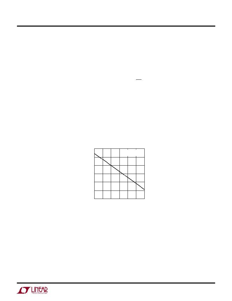
�To� prevent� an� overtemperature� condition� in� high� power�
�applications� Figure� 3� should� be� used� to� determine� the�
�maximum� combination� of� ambient� temperature� and� power�
�1.2�
�1.0�
�0.8�
�0.6�
�0.4�
�0.2�
�dissipation.� The� power� dissipated� in� the� LTC3250-1.5/�
�LTC3250-1.2� should� always� fall� under� the� line� shown� (i.e.�
�within� the� safe� region)� for� a� given� ambient� temperature.�
�The� power� dissipated� in� the� LTC3250-1.5/LTC3250-1.2� is�
�given� by� the� expression:�
�?� V� ?�
�?� 2� ?�
�This� derating� curve� assumes� a� maximum� thermal� resis-�
�tance,� θ� JA� ,� of� 175� °� C/W� for� the� 6-pin� ThinSOT-23.� This�
�thermal� resistances� can� be� achieved� from� a� printed� circuit�
�board� layout� with� a� solid� ground� plane� (2000mm� 2� )on� at�
�least� one� layer� with� a� good� thermal� connection� to� the�
�ground� pin� of� the� LTC3250-1.5/LTC3250-1.2.� Operation�
�outside� of� this� curve� will� cause� the� junction� temperature� to�
�exceed� 140� °� C� which� may� trigger� the� thermal� shutdown�
�circuitry� and� ultimately� reduce� the� life� of� the� device.�
�θ� JA� =� 175� °� C/W�
�T� J� =� 140� °� C�
�0�
�–50�
�–25�
�0� 25� 50�
�75�
�100�
�AMBIENT� TEMPERATURE� (� °� C)�
�3250� ?� F03�
�Figure� 3.� Maximum� Power� Dissipation� vs� Ambient� Temperature�
�3250fa�
�9�
�相关PDF资料 |
PDF描述 |
|---|---|
| LTC3251EMSE-1.5#TRPBF | IC REG BUCK SWITCHED CAP 10MSOP |
| LTC3252EDE#TRPBF | IC REG BUCK SWITCHED CAP 12DFN |
| LTC3388IMSE-3#TRPBF | IC REG BUCK SYNC 50MA 10MSOP |
| LTC3400ES6-1#TRPBF | IC REG BST SYNC ADJ .85A SOT23-6 |
| LTC3401EMS#TR | IC REG BOOST SYNC ADJ 1A 10MSOP |
相关代理商/技术参数 |
参数描述 |
|---|---|
| LTC3251 | 制造商:LINER 制造商全称:Linear Technology 功能描述:500mA High Efficiency, Low Noise, Inductorless Step-Down DC/DC Converter |
| LTC3251-1.2 | 制造商:LINER 制造商全称:Linear Technology 功能描述:500mA High Efficiency, Low Noise, Inductorless Step-Down DC/DC Converter |
| LTC3251-1.5 | 制造商:LINER 制造商全称:Linear Technology 功能描述:500mA High Efficiency, Low Noise, Inductorless Step-Down DC/DC Converter |
| LTC3251EMSE | 功能描述:IC REG BUCK SWITCHED CAP 10MSOP RoHS:否 类别:集成电路 (IC) >> PMIC - 稳压器 - DC DC 开关稳压器 系列:- 标准包装:2,500 系列:- 类型:升压(升压) 输出类型:可调式 输出数:1 输出电压:1.24 V ~ 30 V 输入电压:1.5 V ~ 12 V PWM 型:电流模式,混合 频率 - 开关:600kHz 电流 - 输出:500mA 同步整流器:无 工作温度:-40°C ~ 85°C 安装类型:表面贴装 封装/外壳:8-SOIC(0.154",3.90mm 宽) 包装:带卷 (TR) 供应商设备封装:8-SOIC |
| LTC3251EMSE#PBF | 功能描述:IC REG BUCK SWITCHED CAP 10MSOP RoHS:是 类别:集成电路 (IC) >> PMIC - 稳压器 - DC DC 开关稳压器 系列:- 标准包装:250 系列:- 类型:降压(降压) 输出类型:固定 输出数:1 输出电压:1.2V 输入电压:2.05 V ~ 6 V PWM 型:电压模式 频率 - 开关:2MHz 电流 - 输出:500mA 同步整流器:是 工作温度:-40°C ~ 85°C 安装类型:表面贴装 封装/外壳:6-UFDFN 包装:带卷 (TR) 供应商设备封装:6-SON(1.45x1) 产品目录页面:1032 (CN2011-ZH PDF) 其它名称:296-25628-2 |
发布紧急采购,3分钟左右您将得到回复。