参数资料
| 型号: | LTC3401EMS#TR |
| 厂商: | Linear Technology |
| 文件页数: | 10/16页 |
| 文件大小: | 0K |
| 描述: | IC REG BOOST SYNC ADJ 1A 10MSOP |
| 标准包装: | 2,500 |
| 类型: | 升压(升压) |
| 输出类型: | 可调式 |
| 输出数: | 1 |
| 输出电压: | 2.6 V ~ 5.5 V |
| 输入电压: | 0.5 V ~ 5.5 V |
| PWM 型: | 电流模式,混合 |
| 频率 - 开关: | 3MHz |
| 电流 - 输出: | 1A |
| 同步整流器: | 是 |
| 工作温度: | -40°C ~ 85°C |
| 安装类型: | 表面贴装 |
| 封装/外壳: | 10-TFSOP,10-MSOP(0.118",3.00mm 宽) |
| 包装: | 带卷 (TR) |
| 供应商设备封装: | 10-MSOP |
| 其它名称: | LTC3401EMSTR |
�� �
�
�LTC3401�
�APPLICATIO� S� I� FOR� ATIO�
�In� some� layouts� it� may� be� required� to� place� a� 1� μ� F� low� ESR�
�capacitor� as� close� to� the� V� OUT� and� GND� pins� as� possible.�
�Input� Capacitor� Selection�
�The� input� filter� capacitor� reduces� peak� currents� drawn� from�
�the� input� source� and� reduces� input� switching� noise.� Since�
�the� IC� can� operate� at� voltages� below� 0.5V� once� the� output�
�is� regulated,� demand� on� the� input� capacitor� is� much� less�
�and� in� most� applications� a� 3.3� μ� F� is� sufficient.�
�Output� Diode�
�For� applications� with� output� voltages� over� 4.3V,� a� Schottky�
�diode� is� required� to� ensure� that� the� SW� pin� voltage� does�
�not� exceed� its� absolute� maximum� rating.� The� Schottky�
�diode� across� the� synchronous� PMOS� switch� provides� a�
�lower� drop� during� the� break-before-make� time� (typically�
�20ns)� of� the� NMOS� to� PMOS� transition.� The� Schottky�
�diode� improves� peak� efficiency� (see� graph� “Efficiency�
�Loss� Without� Schottky� vs� Frequency”).� Use� of� a� Schottky�
�diode� such� as� a� MBRM120T3,� 1N5817� or� equivalent.�
�In� this� case,� converter� frequencies� up� to� 3MHz� may� be�
�employed.�
�The� second� consideration� is� the� physical� size� of� the�
�converter.� As� the� operating� frequency� goes� up,� the� induc-�
�tor� and� filter� caps� go� down� in� value� and� size.� The� trade� off�
�is� in� efficiency� since� the� switching� losses� due� to� gate�
�charge� are� going� up� proportional� with� frequency.� For�
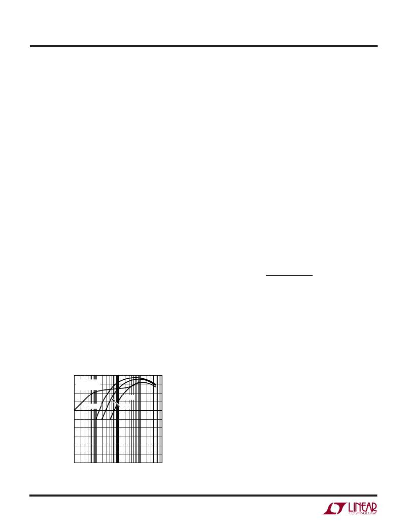
�example� in� Figure� 2,� for� a� 2.4V� to� 3.3V� converter,� the�
�efficiency� at� 100mA� is� 5%� less� at� 2MHz� compared� to�
�300kHz.�
�Another� operating� frequency� consideration� is� whether� the�
�application� can� allow� “pulse� skipping.”� In� this� mode,� the�
�minimum� on� time� of� the� converter� cannot� support� the� duty�
�cycle,� so� the� converter� ripple� will� go� up� and� there� will� be�
�a� low� frequency� component� of� the� output� ripple.� In� many�
�applications� where� physical� size� is� the� main� criterion� then�
�running� the� converter� in� this� mode� is� acceptable.� In�
�applications� where� it� is� preferred� not� to� enter� this� mode,�
�then� the� maximum� operating� frequency� is� given� by:�
�Since� slow� recovery� times� will� compromise� efficiency,� do�
�not� use� ordinary� rectifier� diodes.�
�f� MAX� _� NOSKIP� =�
�V� OUT� –� V� IN�
�V� OUT� ?� t� ON� (� MIN� )�
�Hz�
�Operating� Frequency� Selection�
�There� are� several� considerations� in� selecting� the� operat-�
�ing� frequency� of� the� converter.� The� first� is� determining�
�the� sensitive� frequency� bands� that� cannot� tolerate� any�
�spectral� noise.� For� example,� in� products� incorporating�
�RF� communications,� the� 455kHz� IF� frequency� is� sensitive�
�to� any� noise,� therefore� switching� above� 600kHz� is� de-�
�sired.� Some� communications� have� sensitivity� to� 1.1MHz.�
�100�
�where� t� ON(MIN)� =� minimum� on� time� =� 120ns�
�Reducing� Output� Capacitance� with� a� Load� Feed�
�Forward� Signal�
�In� many� applications� the� output� filter� capacitance� can� be�
�reduced� for� the� desired� transient� response� by� having� the�
�device� commanding� the� change� in� load� current,� (i.e.�
�system� microcontroller),� inform� the� power� converter� of�
�the� changes� as� they� occur.� Specifically,� a� “load� feed�
�90�
�Burst� Mode�
�OPERATION�
�forward”� signal� coupled� into� the� V� C� pin� gives� the� inner�
�80�
�70�
�60�
�50�
�40�
�30�
�20�
�10�
�0�
�0.1�
�3� MHz�
�300kHz 1MHz�
�1� 10� 100�
�OUTPUT� CURRENT� (mA)�
�1000�
�current� loop� a� head� start� in� providing� the� change� in� output�
�current.� The� transconductance� of� the� LTC3401� converter�
�at� the� V� C� pin� with� respect� to� the� inductor� current� is� typically�
�130mA/100mV,� so� the� amount� of� signal� injected� is� pro-�
�portional� to� the� anticipated� change� of� inductor� current�
�with� load.� The� outer� voltage� loop� performs� the� remainder�
�of� the� correction,� but� because� of� the� load� feed� forward�
�signal,� the� range� over� which� it� must� slew� is� greatly�
�reduced.� This� results� in� an� improved� transient� response.�
�3401� G08�
�Figure� 2.� Converter� Efficiency� 2.4V� to� 3.3V�
�3401fb�
�10�
�相关PDF资料 |
PDF描述 |
|---|---|
| LTC3402EMS#TR | IC REG BOOST SYNC ADJ 2A 10MSOP |
| LTC3403EDD#TRPBF | IC REG BUCK SYNC ADJ 0.6A 8DFN |
| LTC3404MPMS8#PBF | IC REG BUCK SYNC ADJ 0.6A 8MSOP |
| LTC3405ES6#TRPBF | IC REG BUCK SYNC ADJ .3A SOT23-6 |
| LTC3406BES5-1.2#TRPBF | IC REG BUCK SYNC 1.2V TSOT23-5 |
相关代理商/技术参数 |
参数描述 |
|---|---|
| LTC3402 | 制造商:LINER 制造商全称:Linear Technology 功能描述:1.2MHz Step-Up DC/DC Converter in SOT-23 |
| LTC3402EMS | 功能描述:IC REG BOOST SYNC ADJ 2A 10MSOP RoHS:否 类别:集成电路 (IC) >> PMIC - 稳压器 - DC DC 开关稳压器 系列:- 标准包装:2,500 系列:- 类型:降压(降压) 输出类型:固定 输出数:1 输出电压:1.2V,1.5V,1.8V,2.5V 输入电压:2.7 V ~ 20 V PWM 型:- 频率 - 开关:- 电流 - 输出:50mA 同步整流器:是 工作温度:-40°C ~ 125°C 安装类型:表面贴装 封装/外壳:10-TFSOP,10-MSOP(0.118",3.00mm 宽)裸露焊盘 包装:带卷 (TR) 供应商设备封装:10-MSOP 裸露焊盘 |
| LTC3402EMS#PBF | 功能描述:IC REG BOOST SYNC ADJ 2A 10MSOP RoHS:是 类别:集成电路 (IC) >> PMIC - 稳压器 - DC DC 开关稳压器 系列:- 标准包装:250 系列:- 类型:降压(降压) 输出类型:固定 输出数:1 输出电压:1.2V 输入电压:2.05 V ~ 6 V PWM 型:电压模式 频率 - 开关:2MHz 电流 - 输出:500mA 同步整流器:是 工作温度:-40°C ~ 85°C 安装类型:表面贴装 封装/外壳:6-UFDFN 包装:带卷 (TR) 供应商设备封装:6-SON(1.45x1) 产品目录页面:1032 (CN2011-ZH PDF) 其它名称:296-25628-2 |
| LTC3402EMS#TR | 功能描述:IC REG BOOST SYNC ADJ 2A 10MSOP RoHS:否 类别:集成电路 (IC) >> PMIC - 稳压器 - DC DC 开关稳压器 系列:- 标准包装:2,500 系列:- 类型:降压(降压) 输出类型:固定 输出数:1 输出电压:1.2V,1.5V,1.8V,2.5V 输入电压:2.7 V ~ 20 V PWM 型:- 频率 - 开关:- 电流 - 输出:50mA 同步整流器:是 工作温度:-40°C ~ 125°C 安装类型:表面贴装 封装/外壳:10-TFSOP,10-MSOP(0.118",3.00mm 宽)裸露焊盘 包装:带卷 (TR) 供应商设备封装:10-MSOP 裸露焊盘 |
| LTC3402EMS#TRPBF | 功能描述:IC REG BOOST SYNC ADJ 2A 10MSOP RoHS:是 类别:集成电路 (IC) >> PMIC - 稳压器 - DC DC 开关稳压器 系列:- 标准包装:2,500 系列:- 类型:降压(降压) 输出类型:固定 输出数:1 输出电压:1.2V,1.5V,1.8V,2.5V 输入电压:2.7 V ~ 20 V PWM 型:- 频率 - 开关:- 电流 - 输出:50mA 同步整流器:是 工作温度:-40°C ~ 125°C 安装类型:表面贴装 封装/外壳:10-TFSOP,10-MSOP(0.118",3.00mm 宽)裸露焊盘 包装:带卷 (TR) 供应商设备封装:10-MSOP 裸露焊盘 |
发布紧急采购,3分钟左右您将得到回复。