- 您现在的位置:买卖IC网 > PDF目录14066 > LTC3404EMS8#TRPBF (Linear Technology)IC REG BUCK SYNC ADJ 0.6A 8MSOP PDF资料下载
参数资料
| 型号: | LTC3404EMS8#TRPBF |
| 厂商: | Linear Technology |
| 文件页数: | 8/16页 |
| 文件大小: | 0K |
| 描述: | IC REG BUCK SYNC ADJ 0.6A 8MSOP |
| 标准包装: | 2,500 |
| 类型: | 降压(降压) |
| 输出类型: | 可调式 |
| 输出数: | 1 |
| 输出电压: | 0.8 V ~ 6 V |
| 输入电压: | 2.65 V ~ 6 V |
| PWM 型: | 电流模式,混合 |
| 频率 - 开关: | 1.4MHz |
| 电流 - 输出: | 600mA |
| 同步整流器: | 是 |
| 工作温度: | -40°C ~ 85°C |
| 安装类型: | 表面贴装 |
| 封装/外壳: | 8-TSSOP,8-MSOP(0.118",3.00mm 宽) |
| 包装: | 带卷 (TR) |
| 供应商设备封装: | 8-MSOP |
�� �
�
�LTC3404�
�OPERATIO�
�When� the� converter� is� in� Burst� Mode� operation,� the� peak�
�current� of� the� inductor� is� set� to� approximately� 250mA,�
�even� though� the� voltage� at� the� I� TH� pin� indicates� a� lower�
�value.� The� voltage� at� the� I� TH� pin� drops� when� the� inductor’s�
�average� current� is� greater� than� the� load� requirement.� As�
�the� I� TH� voltage� drops� below� approximately� 0.55V,� the�
�BURST� comparator� trips,� causing� the� internal� sleep� line� to�
�go� high� and� forces� off� both� power� MOSFETs.� The� I� TH� pin�
�is� then� disconnected� from� the� output� of� the� EA� amplifier�
�and� held� a� diode� voltage� (0.7V)� above� ground.�
�In� sleep� mode,� both� power� MOSFETs� are� held� off� and� a�
�majority� of� the� internal� circuitry� is� partially� turned� off,�
�reducing� the� quiescent� current� to� 10� μ� A.� The� load� current�
�is� now� being� supplied� solely� from� the� output� capacitor.�
�When� the� output� voltage� drops,� the� I� TH� pin� reconnects� to�
�the� output� of� the� EA� amplifier� and� the� top� MOSFET� is� again�
�turned� on� and� this� process� repeats.�
�Short-Circuit� Protection�
�When� the� output� is� shorted� to� ground,� the� frequency� of� the�
�oscillator� is� reduced� to� about� 200kHz,� 1/7� the� nominal�
�frequency.� This� frequency� foldback� ensures� that� the�
�inductor� current� has� ample� time� to� decay,� thereby� prevent-�
�ing� runaway.� The� oscillator’s� frequency� will� progressively�
�increase� to� 1.4MHz� (or� the� synchronized� frequency)� when�
�V� FB� rises� above� 0.3V.�
�Frequency� Synchronization�
�A� phase-locked� loop� (PLL)� is� available� on� the� LTC3404� to�
�allow� the� internal� oscillator� to� be� synchronized� to� an�
�low� audio� noise� and� reduced� RF� interference� while� provid-�
�ing� reasonable� low� current� efficiency.�
�Frequency� synchronization� is� inhibited� when� the� feedback�
�voltage� V� FB� is� below� 0.6V.� This� prevents� the� external� clock�
�from� interfering� with� the� frequency� foldback� for� short-�
�circuit� protection.�
�Dropout� Operation�
�When� the� input� supply� voltage� decreases� toward� the�
�output� voltage,� the� duty� cycle� increases� toward� the� maxi-�
�mum� on-time.� Further� reduction� of� the� supply� voltage�
�forces� the� main� switch� to� remain� on� for� more� than� one�
�cycle� until� it� reaches� 100%� duty� cycle.� The� output� voltage�
�will� then� be� determined� by� the� input� voltage� minus� the�
�voltage� drop� across� the� internal� P-channel� MOSFET� and�
�the� inductor.�
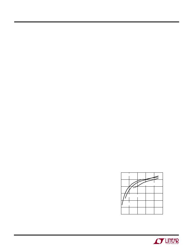
�Low� Supply� Operation�
�The� LTC3404� is� designed� to� operate� down� to� an� input�
�supply� voltage� of� 2.65V� although� the� maximum� allowable�
�output� current� is� reduced� at� this� low� voltage.� Figure� 1�
�shows� the� reduction� in� the� maximum� output� current� as� a�
�function� of� input� voltage� for� various� output� voltages.�
�Another� important� detail� to� remember� is� that� at� low� input�
�supply� voltages,� the� R� DS(ON)� of� the� P-channel� switch�
�increases.� Therefore,� the� user� should� calculate� the� power�
�dissipation� when� the� LTC3404� is� used� at� 100%� duty� cycle�
�with� a� low� input� voltage� (see� Thermal� Considerations� in�
�the� Applications� Information� section).�
�external� source� connected� to� the� SYNC/MODE� pin.� The�
�output� of� the� phase� detector� at� the� PLL� LPF� pin� operates�
�over� a� 0V� to� 2.4V� range� corresponding� to� 1MHz� to� 1.7MHz.�
�When� locked,� the� PLL� aligns� the� turn-on� of� the� top� MOS-�
�1200�
�1000�
�800�
�L = 4.7� μ� H�
�V� OUT� = 3.3V�
�FET� to� the� rising� edge� of� the� synchronizing� signal.�
�600�
�When� the� LTC3404� is� clocked� by� an� external� source,� Burst�
�V� OUT� = 2.5V�
�Mode� operation� is� disabled;� the� LTC3404� then� operates� in�
�PWM� pulse� skipping� mode.� In� this� mode,� when� the� output�
�load� is� very� low,� current� comparator� I� COMP� may� remain�
�400�
�200�
�V� OUT� = 1.5V�
�tripped� for� several� cycles� and� force� the� main� switch� to� stay�
�off� for� the� same� number� of� cycles.� Increasing� the� output�
�0�
�2.5�
�3.5�
�4.5� 5.5� 6.5�
�SUPPLY� VOLTAGE� (V)�
�7.5�
�load� slightly� allows� constant� frequency� PWM� operation� to�
�resume.� This� mode� exhibits� low� output� ripple� as� well� as�
�3404� ?� F01�
�Figure� 1.� Maximum� Output� Current� vs� Input� Voltage�
�3404fb�
�8�
�相关PDF资料 |
PDF描述 |
|---|---|
| ESC19DRYS-S93 | CONN EDGECARD 38POS DIP .100 SLD |
| VI-J6B-EZ | CONVERTER MOD DC/DC 95V 25W |
| 25MS74.7MEFC4X7 | CAP ALUM 4.7UF 25V 20% RADIAL |
| VI-J61-EZ | CONVERTER MOD DC/DC 12V 25W |
| ESC26DREN-S93 | CONN EDGECARD 52POS .100 EYELET |
相关代理商/技术参数 |
参数描述 |
|---|---|
| LTC3404IMS8 | 制造商:Linear Technology 功能描述:DP-SWREG/Monolithic, 1.4MHz High Eff Synch Step-dn Reg |
| LTC3404IMS8#PBF | 功能描述:IC REG BUCK SYNC ADJ 0.6A 8MSOP RoHS:是 类别:集成电路 (IC) >> PMIC - 稳压器 - DC DC 开关稳压器 系列:- 标准包装:2,500 系列:- 类型:降压(降压) 输出类型:固定 输出数:1 输出电压:1.2V,1.5V,1.8V,2.5V 输入电压:2.7 V ~ 20 V PWM 型:- 频率 - 开关:- 电流 - 输出:50mA 同步整流器:是 工作温度:-40°C ~ 125°C 安装类型:表面贴装 封装/外壳:10-TFSOP,10-MSOP(0.118",3.00mm 宽)裸露焊盘 包装:带卷 (TR) 供应商设备封装:10-MSOP 裸露焊盘 |
| LTC3404IMS8#TRPBF | 功能描述:IC REG BUCK SYNC ADJ 0.6A 8MSOP RoHS:是 类别:集成电路 (IC) >> PMIC - 稳压器 - DC DC 开关稳压器 系列:- 标准包装:2,500 系列:- 类型:降压(降压) 输出类型:固定 输出数:1 输出电压:1.2V,1.5V,1.8V,2.5V 输入电压:2.7 V ~ 20 V PWM 型:- 频率 - 开关:- 电流 - 输出:50mA 同步整流器:是 工作温度:-40°C ~ 125°C 安装类型:表面贴装 封装/外壳:10-TFSOP,10-MSOP(0.118",3.00mm 宽)裸露焊盘 包装:带卷 (TR) 供应商设备封装:10-MSOP 裸露焊盘 |
| LTC3404MPMS8 | 制造商:Linear Technology 功能描述:Conv DC-DC Single Step Down 2.65V to 6V 8-Pin MSOP |
| LTC3404MPMS8#PBF | 功能描述:IC REG BUCK SYNC ADJ 0.6A 8MSOP RoHS:是 类别:集成电路 (IC) >> PMIC - 稳压器 - DC DC 开关稳压器 系列:- 设计资源:Design Support Tool 标准包装:1 系列:- 类型:升压(升压) 输出类型:固定 输出数:1 输出电压:3V 输入电压:0.75 V ~ 2 V PWM 型:- 频率 - 开关:- 电流 - 输出:100mA 同步整流器:是 工作温度:-40°C ~ 85°C 安装类型:表面贴装 封装/外壳:SOT-23-5 细型,TSOT-23-5 包装:剪切带 (CT) 供应商设备封装:TSOT-23-5 其它名称:AS1323-BTTT-30CT |
发布紧急采购,3分钟左右您将得到回复。