- 您现在的位置:买卖IC网 > PDF目录14888 > LTC3405ES6#TRMPBF (Linear Technology)IC REG BUCK SYNC ADJ .3A SOT23-6 PDF资料下载
参数资料
| 型号: | LTC3405ES6#TRMPBF |
| 厂商: | Linear Technology |
| 文件页数: | 7/16页 |
| 文件大小: | 0K |
| 描述: | IC REG BUCK SYNC ADJ .3A SOT23-6 |
| 标准包装: | 1 |
| 类型: | 降压(降压) |
| 输出类型: | 可调式 |
| 输出数: | 1 |
| 输出电压: | 0.8 V ~ 6 V |
| 输入电压: | 2.5 V ~ 5.5 V |
| PWM 型: | 电流模式,混合 |
| 频率 - 开关: | 1.5MHz |
| 电流 - 输出: | 300mA |
| 同步整流器: | 是 |
| 工作温度: | -40°C ~ 85°C |
| 安装类型: | 表面贴装 |
| 封装/外壳: | SOT-23-6 细型,TSOT-23-6 |
| 包装: | 标准包装 |
| 供应商设备封装: | TSOT-23-6 |
| 产品目录页面: | 1334 (CN2011-ZH PDF) |
| 其它名称: | LTC3405ES6#TRMPBFDKR |
�� �
�
�LTC3405�
�OPERATIO�
�(Refer� to� Functional� Diagram)�
�Comparator� OVDET� guards� against� transient� overshoots�
�>� 6.25%� by� turning� the� main� switch� off� and� keeping� it� off�
�until� the� fault� is� removed.�
�Burst� Mode� Operation�
�The� LTC3405� is� capable� of� Burst� Mode� operation� in� which�
�the� internal� power� MOSFETs� operate� intermittently� based�
�on� load� demand.� To� enable� Burst� Mode� operation,� simply�
�connect� the� MODE� pin� to� GND.� To� disable� Burst� Mode�
�operation� and� enable� PWM� pulse� skipping� mode,� connect�
�the� MODE� pin� to� V� IN� or� drive� it� with� a� logic� high� (V� MODE� >�
�1.5V).� In� this� mode,� the� efficiency� is� lower� at� light� loads,�
�but� becomes� comparable� to� Burst� Mode� operation� when�
�the� output� load� exceeds� 25mA.� The� advantage� of� pulse�
�skipping� mode� is� lower� output� ripple� and� less� interference�
�to� audio� circuitry.�
�When� the� converter� is� in� Burst� Mode� operation,� the� peak�
�current� of� the� inductor� is� set� to� approximately� 100mA� re-�
�until� it� reaches� 100%� duty� cycle.� The� output� voltage� will� then�
�be� determined� by� the� input� voltage� minus� the� voltage� drop�
�across� the� P-channel� MOSFET� and� the� inductor.�
�Another� important� detail� to� remember� is� that� at� low� input�
�supply� voltages,� the� R� DS(ON)� of� the� P-channel� switch�
�increases� (see� Typical� Performance� Characteristics).� There-�
�fore,� the� user� should� calculate� the� power� dissipation� when�
�the� LTC3405� is� used� at� 100%� duty� cycle� with� low� input�
�voltage� (See� Thermal� Considerations� in� the� Applications�
�Information� section).�
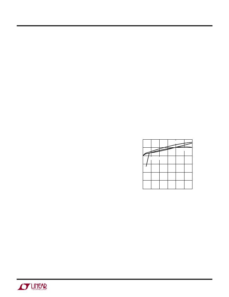
�Low� Supply� Operation�
�The� LTC3405� will� operate� with� input� supply� voltages� as�
�low� as� 2.5V,� but� the� maximum� allowable� output� current� is�
�reduced� at� this� low� voltage.� Figure� 2� shows� the� reduction�
�in� the� maximum� output� current� as� a� function� of� input�
�voltage� for� various� output� voltages.�
�gardless� of� the� output� load.� Each� burst� event� can� last� from�
�a� few� cycles� at� light� loads� to� almost� continuously� cycling�
�with� short� sleep� intervals� at� moderate� loads.� In� between�
�these� burst� events,� the� power� MOSFETs� and� any� unneeded�
�circuitry� are� turned� off,� reducing� the� quiescent� current� to�
�20� μ� A.� In� this� sleep� state,� the� load� current� is� being� supplied�
�solely� from� the� output� capacitor.� As� the� output� voltage�
�droops,� the� EA� amplifier’s� output� rises� above� the� sleep�
�threshold� signaling� the� BURST� comparator� to� trip� and� turn�
�600�
�500�
�400�
�300�
�200�
�100�
�V� OUT� = 2.5V�
�V� OUT� = 1.8V�
�V� OUT� = 1.3V�
�the� top� MOSFET� on.� This� process� repeats� at� a� rate� that� is�
�dependent� on� the� load� demand.�
�0�
�2.5�
�3.0�
�3.5� 4.0� 4.5�
�SUPPLY� VOLTAGE� (V)�
�5.0�
�5.5�
�3405� G23�
�Short-Circuit� Protection�
�When� the� output� is� shorted� to� ground,� the� frequency� of� the�
�oscillator� is� reduced� to� about� 210kHz,� 1/7� the� nominal�
�frequency.� This� frequency� foldback� ensures� that� the� in-�
�ductor� current� has� more� time� to� decay,� thereby� preventing�
�runaway.� The� oscillator’s� frequency� will� progressively�
�increase� to� 1.5MHz� when� V� FB� rises� above� 0V.�
�Dropout� Operation�
�As� the� input� supply� voltage� decreases� to� a� value� approach-�
�ing� the� output� voltage,� the� duty� cycle� increases� toward� the�
�maximum� on-time.� Further� reduction� of� the� supply� voltage�
�forces� the� main� switch� to� remain� on� for� more� than� one� cycle�
�Figure� 2.� Maximum� Output� Current� vs� Input� Voltage�
�Slope� Compensation� and� Inductor� Peak� Current�
�Slope� compensation� provides� stability� in� constant� fre-�
�quency� architectures� by� preventing� subharmonic� oscilla-�
�tions� at� high� duty� cycles.� It� is� accomplished� internally� by�
�adding� a� compensating� ramp� to� the� inductor� current�
�signal� at� duty� cycles� in� excess� of� 40%.� Normally,� this�
�results� in� a� reduction� of� maximum� inductor� peak� current�
�for� duty� cycles� >� 40%.� However,� the� LTC3405� uses� a�
�patent-pending� scheme� that� counteracts� this� compensat-�
�ing� ramp,� which� allows� the� maximum� inductor� peak�
�current� to� remain� unaffected� throughout� all� duty� cycles.�
�3405fa�
�7�
�相关PDF资料 |
PDF描述 |
|---|---|
| VE-JTK-EY-F3 | CONVERTER MOD DC/DC 40V 50W |
| RSM11DRYH-S13 | CONN EDGECARD 22POS .156 EXTEND |
| RBA35DTBS | CONN EDGECARD 70POS R/A .125 SLD |
| RMM11DRYH-S13 | CONN EDGECARD 22POS .156 EXTEND |
| LKS1V392MESY | CAP ALUM 3900UF 35V 20% SNAP |
相关代理商/技术参数 |
参数描述 |
|---|---|
| LTC3406 | 制造商:LINER 制造商全称:Linear Technology 功能描述:1.5MHz, 600mA Synchronous Step-Down Regulator in ThinSOT |
| LTC3406-1.2 | 制造商:LINER 制造商全称:Linear Technology 功能描述:1.5MHz, 600mA Synchronous Step-Down Regulator in ThinSOT |
| LTC3406-1.5 | 制造商:LINER 制造商全称:Linear Technology 功能描述:1.5MHz, 600mA Synchronous Step-Down egulator in ThinSOT |
| LTC3406-1.8 | 制造商:LINER 制造商全称:Linear Technology 功能描述:1.5MHz, 600mA Synchronous Step-Down egulator in ThinSOT |
| LTC3406A | 制造商:LINER 制造商全称:Linear Technology 功能描述:High Efficiency Battery Charger/USB Power Manager |
发布紧急采购,3分钟左右您将得到回复。