- 您现在的位置:买卖IC网 > PDF目录1829 > LTC3406ES5-1.8#TRPBF (Linear Technology)IC REG BUCK SYNC 1.8V TSOT23-5 PDF资料下载
参数资料
| 型号: | LTC3406ES5-1.8#TRPBF |
| 厂商: | Linear Technology |
| 文件页数: | 7/16页 |
| 文件大小: | 0K |
| 描述: | IC REG BUCK SYNC 1.8V TSOT23-5 |
| 标准包装: | 2,500 |
| 类型: | 降压(降压) |
| 输出类型: | 固定 |
| 输出数: | 1 |
| 输出电压: | 1.8V |
| 输入电压: | 2.5 V ~ 5.5 V |
| PWM 型: | 电流模式,混合 |
| 频率 - 开关: | 1.5MHz |
| 电流 - 输出: | 600mA |
| 同步整流器: | 是 |
| 工作温度: | -40°C ~ 85°C |
| 安装类型: | 表面贴装 |
| 封装/外壳: | SOT-23-5 细型,TSOT-23-5 |
| 包装: | 带卷 (TR) |
| 供应商设备封装: | TSOT-23-5 |
�� �
�
�LTC3406�
�LTC3406-1.5/LTC3406-1.8�
�OPERATIO�
�(Refer� to� Functional� Diagram)�
�Short-Circuit� Protection�
�When� the� output� is� shorted� to� ground,� the� frequency� of� the�
�oscillator� is� reduced� to� about� 210kHz,� 1/7� the� nominal�
�frequency.� This� frequency� foldback� ensures� that� the� in-�
�ductor� current� has� more� time� to� decay,� thereby� preventing�
�runaway.� The� oscillator’s� frequency� will� progressively�
�increase� to� 1.5MHz� when� V� FB� or� V� OUT� rises� above� 0V.�
�Dropout� Operation�
�As� the� input� supply� voltage� decreases� to� a� value� approach-�
�ing� the� output� voltage,� the� duty� cycle� increases� toward� the�
�maximum� on-time.� Further� reduction� of� the� supply� voltage�
�forces� the� main� switch� to� remain� on� for� more� than� one� cycle�
�until� it� reaches� 100%� duty� cycle.� The� output� voltage� will� then�
�be� determined� by� the� input� voltage� minus� the� voltage� drop�
�across� the� P-channel� MOSFET� and� the� inductor.�
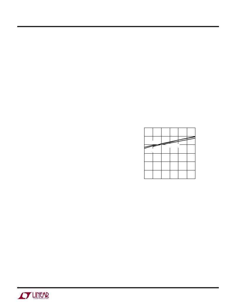
�An� important� detail� to� remember� is� that� at� low� input� supply�
�in� the� maximum� output� current� as� a� function� of� input�
�voltage� for� various� output� voltages.�
�Slope� Compensation� and� Inductor� Peak� Current�
�Slope� compensation� provides� stability� in� constant� fre-�
�quency� architectures� by� preventing� subharmonic� oscilla-�
�tions� at� high� duty� cycles.� It� is� accomplished� internally� by�
�adding� a� compensating� ramp� to� the� inductor� current�
�signal� at� duty� cycles� in� excess� of� 40%.� Normally,� this�
�results� in� a� reduction� of� maximum� inductor� peak� current�
�for� duty� cycles� >� 40%.� However,� the� LTC3406� uses� a�
�patent-pending� scheme� that� counteracts� this� compensat-�
�ing� ramp,� which� allows� the� maximum� inductor� peak�
�current� to� remain� unaffected� throughout� all� duty� cycles.�
�1200�
�1000�
�voltages,� the� R� DS(ON)� of� the� P-channel� switch� increases�
�(see� Typical� Performance� Characteristics).� Therefore,� the�
�user� should� calculate� the� power� dissipation� when� the�
�800�
�600�
�V� OUT� = 1.8V�
�V� OUT� = 1.5V�
�V� OUT� = 2.5V�
�LTC3406� is� used� at� 100%� duty� cycle� with� low� input� voltage�
�(See� Thermal� Considerations� in� the� Applications� Informa-�
�tion� section).�
�400�
�200�
�Low� Supply� Operation�
�0�
�2.5�
�3.0�
�3.5� 4.0� 4.5�
�5.0�
�5.5�
�The� LTC3406� will� operate� with� input� supply� voltages� as�
�low� as� 2.5V,� but� the� maximum� allowable� output� current� is�
�SUPPLY� VOLTAGE� (V)�
�3406� F02�
�reduced� at� this� low� voltage.� Figure� 2� shows� the� reduction�
�Figure� 2.� Maximum� Output� Current� vs� Input� Voltage�
�3406fa�
�7�
�相关PDF资料 |
PDF描述 |
|---|---|
| LTC3407EDD#TRPBF | IC REG BUCK SYNC ADJ 1A DL 10DFN |
| LTC3408EDD#TRPBF | IC REG BUCK W/BYPASS TXRX 8-DFN |
| LTC3409IDD#TRPBF | IC REG BUCK SYNC ADJ 0.6A 8DFN |
| LTC3410BESC6-1.8#TRPBF | IC REG BUCK SYNC 1.8V .3A SC70-6 |
| LTC3411AIMS#TRPBF | IC REG BUCK SYNC ADJ 10MSOP |
相关代理商/技术参数 |
参数描述 |
|---|---|
| LTC3406ES5TRMPBF | 制造商:Linear Technology 功能描述:LTC3406 adj 600mA SD dc-dc converter |
| LTC3407 | 制造商:LINER 制造商全称:Linear Technology 功能描述:Dual Synchronous, 600mA, 1.5MHz Step-Down DC/DC Regulator |
| LTC3407-2 | 制造商:LINER 制造商全称:Linear Technology 功能描述:Monolithic Dual Tracking 3A Step-Down Switching |
| LTC3407-3 | 制造商:LINER 制造商全称:Linear Technology 功能描述:Dual Synchronous, 1.8V/0.8A and 3.3V/0.8A 2.25MHz Step-Down DC/DC Regulator |
| LTC3407-4 | 制造商:LINER 制造商全称:Linear Technology 功能描述:Dual Synchronous, 800mA, 2.25MHz Step-Down DC/DC Regulator |
发布紧急采购,3分钟左右您将得到回复。