- 您现在的位置:买卖IC网 > PDF目录14841 > LTC3409EDD#PBF (Linear Technology)IC REG BUCK SYNC ADJ 0.6A 8DFN PDF资料下载
参数资料
| 型号: | LTC3409EDD#PBF |
| 厂商: | Linear Technology |
| 文件页数: | 12/16页 |
| 文件大小: | 0K |
| 描述: | IC REG BUCK SYNC ADJ 0.6A 8DFN |
| 标准包装: | 121 |
| 类型: | 降压(降压) |
| 输出类型: | 可调式 |
| 输出数: | 1 |
| 输出电压: | 0.62 V ~ 5.5 V |
| 输入电压: | 1.6 V ~ 5.5 V |
| PWM 型: | 电流模式,混合 |
| 频率 - 开关: | 1.7MHz ~ 2.6MHz |
| 电流 - 输出: | 600mA |
| 同步整流器: | 是 |
| 工作温度: | -40°C ~ 85°C |
| 安装类型: | 表面贴装 |
| 封装/外壳: | 8-WFDFN 裸露焊盘 |
| 包装: | 管件 |
| 供应商设备封装: | 8-DFN-EP(3x3) |
| 产品目录页面: | 1334 (CN2011-ZH PDF) |
�� �
�
�LTC3409�
�APPLICATIONS� INFORMATION�
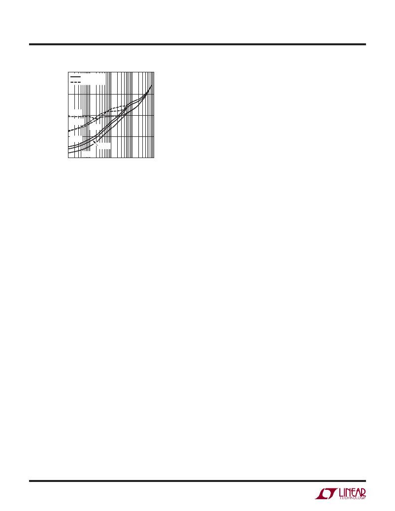
�1�
�BURST�
�Other� losses� including� C� IN� and� C� OUT� ESR� dissipative� losses�
�0.1�
�PULSE� SKIP�
�and� inductor� core� losses� generally� account� for� less� than�
�2%� total� additional� loss.�
�0.01�
�2.5V� IN�
�Thermal� Considerations�
�3.6V� IN�
�4.2V� IN�
�In� most� applications� the� LTC3409� does� not� dissipate� much�
�heat� due� to� its� high� ef?ciency.� But,� in� applications� where� the�
�4.2V� IN�
�0.001�
�0.0001�
�0.1�
�3.6V� IN�
�2.5V� IN�
�1� 10� 100�
�LOAD� CURRENT� (mA)�
�Figure� 2�
�1000�
�3409� F02�
�LTC3409� is� running� at� high� ambient� temperature� with� low�
�supply� voltage� and� high� duty� cycles,� such� as� in� dropout,�
�the� heat� dissipated� may� exceed� the� maximum� junction�
�temperature� of� the� part.� If� the� junction� temperature� reaches�
�approximately� 150°C,� both� power� switches� will� be� turned�
�off� and� the� SW� node� will� become� high� impedance.�
�1.� The� V� IN� quiescent� current� is� due� to� two� components:�
�the� DC� bias� current� as� given� in� the� Electrical� Charac-�
�teristics� and� the� internal� main� switch� and� synchronous�
�switch� gate� charge� currents.� The� gate� charge� current�
�results� from� switching� the� gate� capacitance� of� the�
�internal� power� MOSFET� switches.� Each� time� the� gate�
�is� switched� from� high� to� low� to� high� again,� a� packet�
�of� charge,� dQ,� moves� from� V� IN� to� ground.� The� result-�
�ing� dQ/dt� is� the� current� out� of� V� IN� that� is� typically�
�larger� than� the� DC� bias� current.� In� continuous� mode,�
�I� GATECHG� =� f(Q� T� +� Q� B� )� where� Q� T� and� Q� B� are� the� gate�
�charges� of� the� internal� top� and� bottom� switches.� Both�
�the� DC� bias� and� gate� charge� losses� are� proportional� to�
�V� IN� and� thus� their� effects� will� be� more� pronounced� at�
�higher� supply� voltages.�
�To� avoid� the� LTC3409� from� exceeding� the� maximum�
�junction� temperature,� the� user� will� need� to� do� a� thermal�
�analysis.� The� goal� of� the� thermal� analysis� is� to� determine�
�whether� the� operating� conditions� exceed� the� maximum�
�junction� temperature� of� the� part.� The� temperature� rise� is�
�given� by:�
�T� R� =� (P� D� )(� θ� JA� )�
�where� P� D� is� the� power� dissipated� by� the� regulator� and� θ� JA�
�is� the� thermal� resistance� from� the� junction� of� the� die� to�
�the� ambient� temperature.�
�The� junction� temperature,� T� J� ,� is� given� by:�
�T� J� =� T� A� +� T� R�
�where� T� A� is� the� ambient� temperature.�
�2.�
�I� 2� R�
�losses� are� calculated� from� the� resistances� of� the�
�As� an� example,� consider� the� LTC3409� in� dropout� at� an�
�internal� switches,� R� SW� ,� and� external� inductor� R� L� .� In�
�continuous� mode,� the� average� output� current� ?owing�
�through� inductor� L� is� “chopped”� between� the� main�
�switch� and� the� synchronous� switch.� Thus,� the� series�
�resistance� looking� into� the� SW� pin� is� a� function� of� both�
�top� and� bottom� MOSFET� R� DS(ON)� and� the� duty� cycle�
�(DC)� as� follows:�
�R� SW� =� (R� DS(ON)TOP� )(DC)� +� (R� DS(ON)BOT� )(1� –� DC)�
�The� R� DS(ON)� for� both� the� top� and� bottom� MOSFETs� can� be�
�obtained� from� the� Typical� Performance� Characteristics.�
�Thus,� to� obtain� I� 2� R� losses,� simply� add� R� SW� to� R� L� and�
�multiply� the� result� by� the� square� of� the� average� output�
�input� voltage� of� 1.6V,� a� load� current� of� 600mA� and� an�
�ambient� temperature� of� 75°C.� From� the� typical� perfor-�
�mance� graph� of� switch� resistance,� the� R� DS(ON)� of� the�
�P-channel� switch� at� 75°C� is� approximately� 0.48Ω.� There-�
�fore,� power� dissipated� by� the� part� is:�
�P� D� =� I� LOAD2� ?� R� DS(ON)� =� 172.8mW�
�For� the� DD8� package,� the� θ� JA� is� 43°C/W.� Thus,� the� junction�
�temperature� of� the� regulator� is:�
�T� J� =� 75°C� +� (0.1728)(43)� =� 82.4°C�
�which� is� well� below� the� maximum� junction� temperature�
�of� 125°C.�
�current.�
�3409fc�
�12�
�相关PDF资料 |
PDF描述 |
|---|---|
| LTC3499EDD#PBF | IC REG BOOST SYNC ADJ 0.75A 8DFN |
| EEC44DRXS-S734 | CONN EDGECARD 88POS DIP .100 SLD |
| ISC1812EB471J | INDUCTOR WW 470UH 5% 1812 |
| EMC07DRTI-S734 | CONN EDGECARD 14POS DIP .100 SLD |
| ADP2164ACPZ-R7 | IC REG BUCK SYNC ADJ 4A 16LFCSP |
相关代理商/技术参数 |
参数描述 |
|---|---|
| LTC3409IDD#PBF | 功能描述:IC REG BUCK SYNC ADJ 0.6A 8DFN RoHS:是 类别:集成电路 (IC) >> PMIC - 稳压器 - DC DC 开关稳压器 系列:- 标准包装:2,500 系列:- 类型:降压(降压) 输出类型:固定 输出数:1 输出电压:1.2V,1.5V,1.8V,2.5V 输入电压:2.7 V ~ 20 V PWM 型:- 频率 - 开关:- 电流 - 输出:50mA 同步整流器:是 工作温度:-40°C ~ 125°C 安装类型:表面贴装 封装/外壳:10-TFSOP,10-MSOP(0.118",3.00mm 宽)裸露焊盘 包装:带卷 (TR) 供应商设备封装:10-MSOP 裸露焊盘 |
| LTC3409IDD#TRPBF | 功能描述:IC REG BUCK SYNC ADJ 0.6A 8DFN RoHS:是 类别:集成电路 (IC) >> PMIC - 稳压器 - DC DC 开关稳压器 系列:- 标准包装:2,500 系列:- 类型:降压(降压) 输出类型:固定 输出数:1 输出电压:1.2V,1.5V,1.8V,2.5V 输入电压:2.7 V ~ 20 V PWM 型:- 频率 - 开关:- 电流 - 输出:50mA 同步整流器:是 工作温度:-40°C ~ 125°C 安装类型:表面贴装 封装/外壳:10-TFSOP,10-MSOP(0.118",3.00mm 宽)裸露焊盘 包装:带卷 (TR) 供应商设备封装:10-MSOP 裸露焊盘 |
| LTC3410 | 制造商:LINER 制造商全称:Linear Technology 功能描述:2.25MHz, 300mA Synchronous Step-Down Regulator in SC70 |
| LTC3410-1.875 | 制造商:LINER 制造商全称:Linear Technology 功能描述:2.25MHz, 300mA Synchronous Step-Down Regulator in SC70 |
| LTC3410B | 制造商:LINER 制造商全称:Linear Technology 功能描述:2.25MHz, 300mA Synchronous Step-Down Regulator in SC70 |
发布紧急采购,3分钟左右您将得到回复。