参数资料
| 型号: | LTC3411AIMS#TRPBF |
| 厂商: | Linear Technology |
| 文件页数: | 14/22页 |
| 文件大小: | 0K |
| 描述: | IC REG BUCK SYNC ADJ 10MSOP |
| 标准包装: | 2,500 |
| 类型: | 降压(降压) |
| 输出类型: | 可调式 |
| 输出数: | 1 |
| 输出电压: | 0.8 V ~ 5 V |
| 输入电压: | 2.5 V ~ 5.5 V |
| PWM 型: | 电流模式,混合 |
| 频率 - 开关: | 2.5MHz |
| 电流 - 输出: | 1.25A |
| 同步整流器: | 是 |
| 工作温度: | -40°C ~ 125°C |
| 安装类型: | 表面贴装 |
| 封装/外壳: | 10-TFSOP,10-MSOP(0.118",3.00mm 宽) |
| 包装: | 带卷 (TR) |
| 供应商设备封装: | 10-MSOP |
�� �
�
�LTC3411A�
�APPLICATIONS� INFORMATION�
�pin.� This� prevents� the� output� from� discharging� to� below�
�the� regulation� point� when� soft-starting.�
�Mode� Selection� and� Frequency� Synchronization�
�The� SYNC/MODE� pin� is� a� multipurpose� pin� which� provides�
�mode� selection� and� frequency� synchronization.� Connect-�
�ing� this� pin� to� V� IN� enables� Burst� Mode� operation,� which�
�provides� the� best� low� current� efficiency� at� the� cost� of� a�
�higher� output� voltage� ripple.� When� this� pin� is� connected� to�
�ground,� pulse� skipping� operation� is� selected� which� provides�
�the� lowest� output� voltage� and� current� ripple� at� the� cost�
�of� low� current� efficiency.� Applying� a� voltage� that� is� half�
�the� value� of� the� input� voltage� results� in� forced� continuous�
�mode,� which� creates� a� fixed� output� ripple� and� is� capable� of�
�sinking� up� to� 0.4A.� Since� the� switching� noise� is� constant�
�in� this� mode,� it� is� also� the� easiest� to� filter� out.�
�The� LTC3411A� can� also� be� synchronized� to� an� external�
�clock� signal� by� the� SYNC/MODE� pin.� The� internal� oscilla-�
�tor� frequency� should� be� set� to� ±20%� of� the� external� clock�
�frequency� to� ensure� adequate� slope� compensation,� since�
�slope� compensation� is� derived� from� the� internal� oscillator.�
�During� synchronization,� the� mode� is� set� to� pulse� skipping�
�and� the� top� switch� turn� on� is� synchronized� to� the� falling�
�edge� of� the� external� clock.�
�Checking� Transient� Response�
�The� OPTI-LOOP� ?� compensation� allows� the� transient� re-�
�sponse� to� be� optimized� for� a� wide� range� of� loads� and� output�
�capacitors.� The� availability� of� the� I� TH� pin� not� only� allows�
�optimization� of� the� control� loop� behavior� but� also� provides�
�a� DC� coupled� and� AC� filtered� closed� loop� response� test�
�point.� The� DC� step,� rise� time� and� settling� time� at� this� test�
�point� truly� reflects� the� closed� loop� response.� Assuming� a�
�predominantly� second� order� system,� phase� margin� and/or�
�damping� factor� can� be� estimated� using� the� percentage� of�
�overshoot� seen� at� this� pin.� The� bandwidth� can� also� be�
�estimated� by� examining� the� rise� time� at� the� pin.�
�The� I� TH� external� components� shown� in� the� circuit� on� the�
�front� page� of� this� data� sheet� will� provide� an� adequate� starting�
�point� for� most� applications.� The� series� R-C� filter� sets� the�
�dominant� pole-zero� loop� compensation.� The� values� can�
�be� modified� slightly� (from� 0.5� to� 2� times� their� suggested�
�values)� to� optimize� transient� response� once� the� final� PC�
�layout� is� done� and� the� particular� output� capacitor� type� and�
�value� have� been� determined.� The� output� capacitors� need� to�
�be� selected� because� the� various� types� and� values� determine�
�the� loop� feedback� factor� gain� and� phase.� An� output� current�
�pulse� of� 20%� to� 100%� of� full� load� current� having� a� rise�
�time� of� 1μs� to� 10μs� will� produce� output� voltage� and� I� TH�
�pin� waveforms� that� will� give� a� sense� of� the� overall� loop�
�stability� without� breaking� the� feedback� loop.�
�Switching� regulators� take� several� cycles� to� respond� to� a�
�step� in� load� current.� When� a� load� step� occurs,� V� OUT� imme-�
�diately� shifts� by� an� amount� equal� to� Δ� I� LOAD� ?� ESR,� where�
�ESR� is� the� effective� series� resistance� of� C� OUT� .� Δ� I� LOAD� also�
�begins� to� charge� or� discharge� C� OUT� generating� a� feedback�
�error� signal� used� by� the� regulator� to� return� V� OUT� to� its�
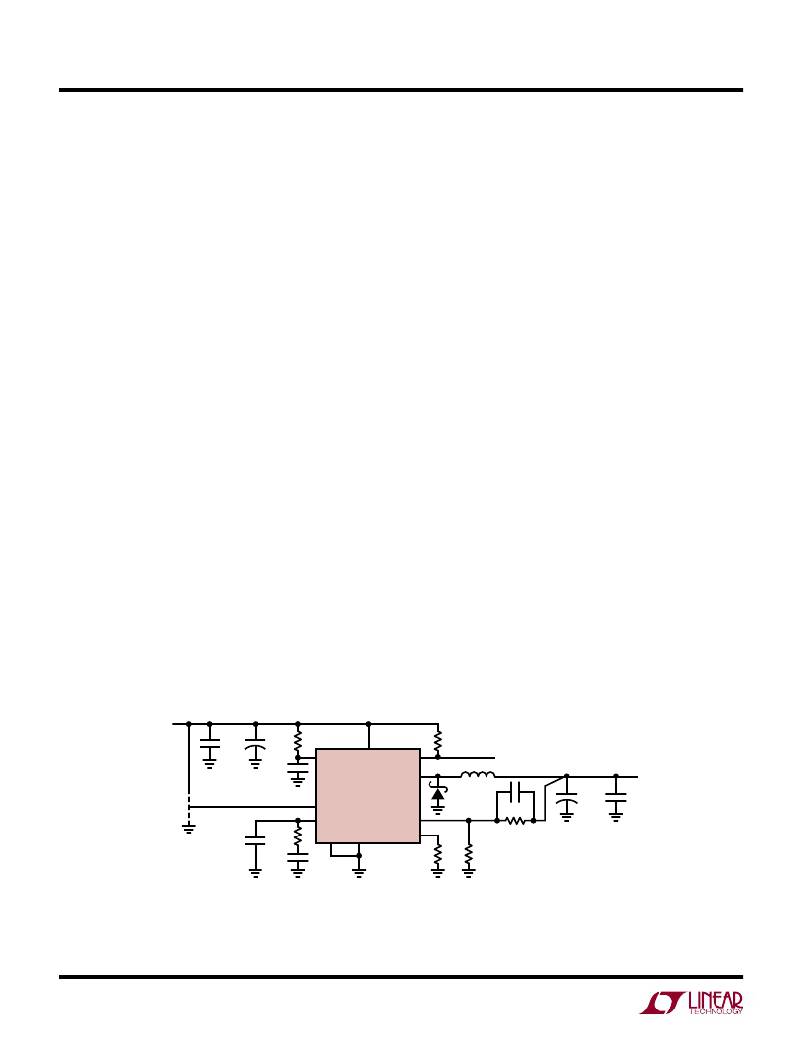
�V� IN�
�C6�
�+�
�C� IN�
�R6�
�R5�
�PGND�
�SGND�
�C� ITH�
�PGND�
�C8�
�SGND�
�R� C�
�SV� IN� PV� IN� PGOOD�
�LTC3411A�
�SYNC/MODE�
�I� TH� V� FB�
�SGND� PGND� SHDN/R� T�
�SW�
�L1�
�D1�
�OPTIONAL�
�PGOOD�
�C� F�
�R2�
�+�
�PGND�
�C� OUT�
�PGND�
�C5�
�V� OUT�
�C� C�
�R� T�
�R1�
�3411A� F05�
�SGND�
�SGND�
�GND�
�SGND� SGND�
�Figure� 5.� LTC3411A� General� Schematic�
�3411afc�
�14�
�For� more� information� www.linear.com/LTC3411A�
�相关PDF资料 |
PDF描述 |
|---|---|
| LTC3411IMS#TRPBF | IC REG BUCK SYNC ADJ 10MSOP |
| LTC3412IFE#TRPBF | IC REG BUCK SYNC ADJ 16TSSOP |
| LTC3413IFE#TRPBF | IC REG BUCK SYNC ADJ 3A 16TSSOP |
| LTC3414MPFE#TRPBF | IC REG BUCK SYNC ADJ 4A 20TSSOP |
| LTC3415EUHF#TRPBF | IC REG BUCK SYNC ADJ 7A 38QFN |
相关代理商/技术参数 |
参数描述 |
|---|---|
| LTC3411EDD | 功能描述:IC REG BUCK SYNC ADJ 1.25A 10DFN RoHS:否 类别:集成电路 (IC) >> PMIC - 稳压器 - DC DC 开关稳压器 系列:- 标准包装:2,500 系列:- 类型:降压(降压) 输出类型:固定 输出数:1 输出电压:1.2V,1.5V,1.8V,2.5V 输入电压:2.7 V ~ 20 V PWM 型:- 频率 - 开关:- 电流 - 输出:50mA 同步整流器:是 工作温度:-40°C ~ 125°C 安装类型:表面贴装 封装/外壳:10-TFSOP,10-MSOP(0.118",3.00mm 宽)裸露焊盘 包装:带卷 (TR) 供应商设备封装:10-MSOP 裸露焊盘 |
| LTC3411EDD#PBF | 功能描述:IC REG BUCK SYNC ADJ 1.25A 10DFN RoHS:是 类别:集成电路 (IC) >> PMIC - 稳压器 - DC DC 开关稳压器 系列:- 标准包装:250 系列:- 类型:降压(降压) 输出类型:固定 输出数:1 输出电压:1.2V 输入电压:2.05 V ~ 6 V PWM 型:电压模式 频率 - 开关:2MHz 电流 - 输出:500mA 同步整流器:是 工作温度:-40°C ~ 85°C 安装类型:表面贴装 封装/外壳:6-UFDFN 包装:带卷 (TR) 供应商设备封装:6-SON(1.45x1) 产品目录页面:1032 (CN2011-ZH PDF) 其它名称:296-25628-2 |
| LTC3411EDD#PBF | 制造商:Linear Technology 功能描述:DC/DC Converter IC |
| LTC3411EDD#TR | 功能描述:IC REG BUCK SYNC ADJ 1.25A 10DFN RoHS:否 类别:集成电路 (IC) >> PMIC - 稳压器 - DC DC 开关稳压器 系列:- 标准包装:2,500 系列:- 类型:降压(降压) 输出类型:固定 输出数:1 输出电压:1.2V,1.5V,1.8V,2.5V 输入电压:2.7 V ~ 20 V PWM 型:- 频率 - 开关:- 电流 - 输出:50mA 同步整流器:是 工作温度:-40°C ~ 125°C 安装类型:表面贴装 封装/外壳:10-TFSOP,10-MSOP(0.118",3.00mm 宽)裸露焊盘 包装:带卷 (TR) 供应商设备封装:10-MSOP 裸露焊盘 |
| LTC3411EDD#TRPBF | 功能描述:IC REG BUCK SYNC ADJ 1.25A 10DFN RoHS:是 类别:集成电路 (IC) >> PMIC - 稳压器 - DC DC 开关稳压器 系列:- 标准包装:2,500 系列:- 类型:降压(降压) 输出类型:固定 输出数:1 输出电压:1.2V,1.5V,1.8V,2.5V 输入电压:2.7 V ~ 20 V PWM 型:- 频率 - 开关:- 电流 - 输出:50mA 同步整流器:是 工作温度:-40°C ~ 125°C 安装类型:表面贴装 封装/外壳:10-TFSOP,10-MSOP(0.118",3.00mm 宽)裸露焊盘 包装:带卷 (TR) 供应商设备封装:10-MSOP 裸露焊盘 |
发布紧急采购,3分钟左右您将得到回复。