- 您现在的位置:买卖IC网 > PDF目录1829 > LTC3417AIFE-2#TRPBF (Linear Technology)IC REG BUCK SYNC ADJ DL 20TSSOP PDF资料下载
参数资料
| 型号: | LTC3417AIFE-2#TRPBF |
| 厂商: | Linear Technology |
| 文件页数: | 18/20页 |
| 文件大小: | 0K |
| 描述: | IC REG BUCK SYNC ADJ DL 20TSSOP |
| 标准包装: | 2,500 |
| 类型: | 降压(降压) |
| 输出类型: | 可调式 |
| 输出数: | 2 |
| 输出电压: | 0.8 V ~ 5 V |
| 输入电压: | 2.25 V ~ 5.5 V |
| PWM 型: | 电流模式,混合 |
| 频率 - 开关: | 1.5MHz,600kHz ~ 4MHz |
| 电流 - 输出: | 1A,1.5A |
| 同步整流器: | 是 |
| 工作温度: | -40°C ~ 125°C |
| 安装类型: | 表面贴装 |
| 封装/外壳: | 20-TSSOP(0.173",4.40mm 宽)裸露焊盘 |
| 包装: | 带卷 (TR) |
| 供应商设备封装: | 20-TSSOP-EP |
�� �
�
�LTC3417A-2�
�APPLICATIONS� INFORMATION�
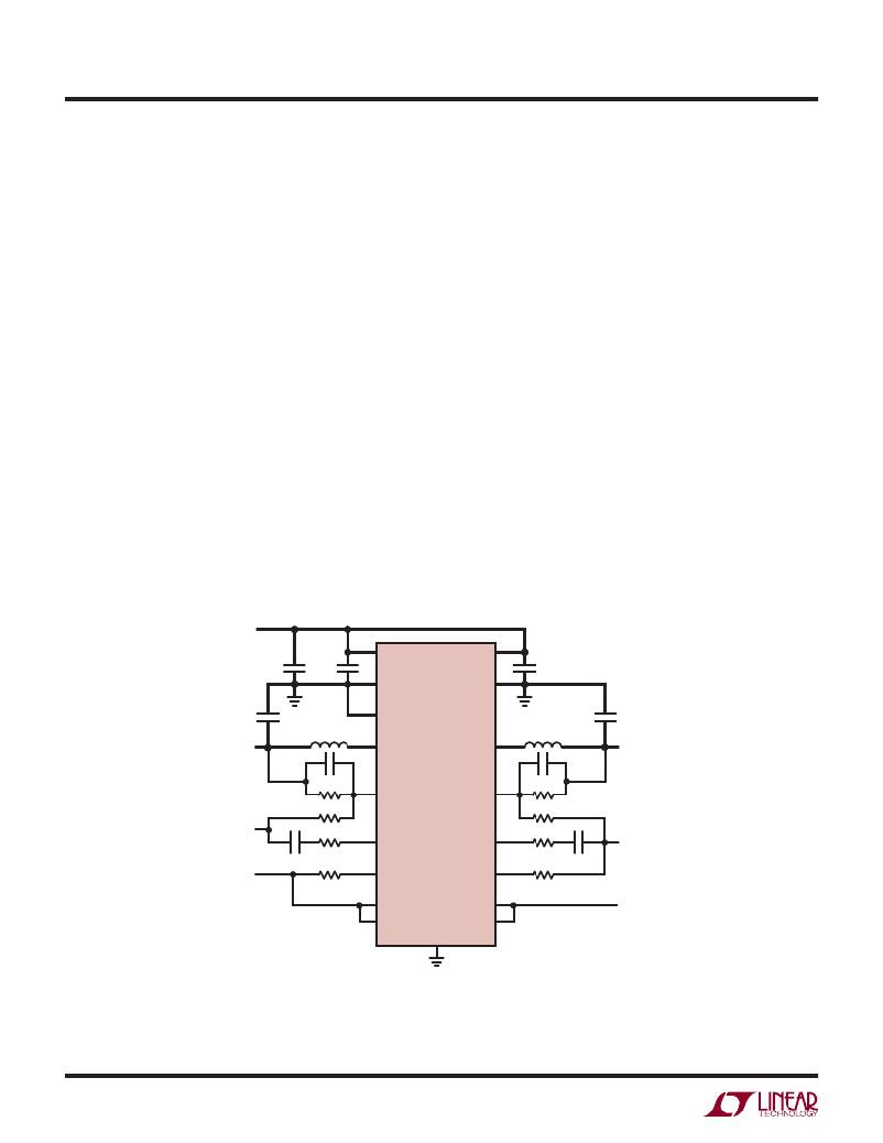
�Board� Layout� Considerations�
�When� laying� out� the� printed� circuit� board,� the� following�
�checklist� should� be� used� to� ensure� proper� operation� of� the�
�LTC3417A-2.� These� items� are� also� illustrated� graphically�
�in� the� layout� diagram� of� Figure� 5.� Check� the� following� in�
�your� layout.�
�1.� Does� the� capacitor� C� IN� connect� to� the� power� V� IN1�
�(Pin� 2),� V� IN2� (Pin� 8),� and� PGND2/GNDD� (Pin� 17)� as�
�close� as� possible� (DFN� package)?� It� may� be� necessary�
�to� split� C� IN� into� two� capacitors.� This� capacitor� provides�
�the� AC� current� to� the� internal� power� MOSFETs� and�
�their� drivers.�
�2.� Are� the� C� OUT1� ,� L� 1� and� C� OUT2� ,� L� 2� closely� connected?� The�
�(–)� plate� of� C� OUT1� returns� current� to� PGND1,� and� the�
�(–)� plate� of� C� OUT2� returns� current� to� the� PGND2/GNDD�
�and� the� (–)� plate� of� C� IN� .�
�3.� The� resistor� divider,� R1� and� R2,� must� be� connected�
�between� the� (+)� plate� of� C� OUT1� and� a� ground� line� ter-�
�minated� near� GNDA.� The� resistor� divider,� R3� and� R4,�
�V� IN�
�must� be� connected� between� the� (+)� plate� of� C� OUT2� and�
�a� ground� line� terminated� near� GNDA.� The� feedback�
�signals� V� FB1� and� V� FB2� should� be� routed� away� from� noise�
�components� and� traces,� such� as� the� SW� lines,� and� its�
�trace� should� be� minimized.�
�4.� Keep� sensitive� components� away� from� the� SW� pins.�
�The� input� capacitor� C� IN� ,� the� compensation� capacitors�
�C� C1� ,� C� C2� ,� C� ITH1� and� C� ITH2� and� all� resistors� R1,� R2,� R3,�
�R4,� R� ITH1� and� R� ITH2� should� be� routed� away� from� the�
�SW� traces� and� the� inductors� L1� and� L2.�
�5.� A� ground� plane� is� preferred,� but� if� not� available,� keep�
�the� signal� and� power� grounds� segregated� with� small�
�signal� components� returning� to� the� GNDA� pin� at� one�
�point� which� is� then� connected� to� the� PGND2/GNDD�
�pin.�
�6.� Flood� all� unused� areas� on� all� layers� with� copper.� Flooding�
�with� copper� will� reduce� the� temperature� rise� of� power�
�components.� These� copper� areas� should� be� connected�
�to� one� of� the� input� supplies.�
�C� OUT2�
�C� IN�
�10μF�
�C� IN2�
�0.1μF�
�V� IN2�
�PGND2/�
�EXPOSED� PAD�
�GNDA�
�V� IN1�
�PGND1�
�C� IN1�
�0.1μF�
�C� OUT1�
�L2�
�L1�
�V� OUT2�
�C� C2�
�R3�
�SW2�
�V� FB2�
�LTC3417A-2�
�SW1�
�V� FB1�
�R1�
�C� C1�
�V� OUT1�
�R4�
�R2�
�STAR� TO�
�GNDA�
�R� ITH2�
�I� TH2�
�I� TH1�
�R� ITH1�
�STAR� TO�
�GNDA�
�V� IN�
�C� ITH2�
�R8�
�POR�
�FREQ�
�R7�
�C� ITH1�
�RUN2�
�PHASE�
�RUN1�
�SYNC/MODE�
�V� IN�
�GNDD�
�3417A-2� F05�
�Figure� 5.� Layout� Guideline�
�3417a2fa�
�18�
�相关PDF资料 |
PDF描述 |
|---|---|
| LTC3417EDHC#PBF | IC REG BUCK SYNC ADJ DL 16DFN |
| LTC3418EUHF#TRPBF | IC REG BUCK SYNC ADJ 8A 38QFN |
| LTC3419IMS-1#TRPBF | IC REG BUCK SYNC ADJ 0.6A 10MSOP |
| LTC3421EUF#TRPBF | IC REG BOOST SYNC ADJ 1.5A 24QFN |
| LTC3422EDD#TRPBF | IC REG BOOST SYNC ADJ 1.5A 10DFN |
相关代理商/技术参数 |
参数描述 |
|---|---|
| LTC3417AIFEPBF | 制造商:Linear Technology 功能描述:Conv DC-DC Dual Step-Down 5.5V TSSOP20EP |
| LTC3417EDHC | 制造商:Linear Technology 功能描述:Conv DC-DC Dual Step Down 2.25V to 5.5V 16-Pin DFN EP |
| LTC3417EDHC#PBF | 功能描述:IC REG BUCK SYNC ADJ DL 16DFN RoHS:是 类别:集成电路 (IC) >> PMIC - 稳压器 - DC DC 开关稳压器 系列:- 设计资源:Design Support Tool 标准包装:1 系列:- 类型:升压(升压) 输出类型:固定 输出数:1 输出电压:3V 输入电压:0.75 V ~ 2 V PWM 型:- 频率 - 开关:- 电流 - 输出:100mA 同步整流器:是 工作温度:-40°C ~ 85°C 安装类型:表面贴装 封装/外壳:SOT-23-5 细型,TSOT-23-5 包装:剪切带 (CT) 供应商设备封装:TSOT-23-5 其它名称:AS1323-BTTT-30CT |
| LTC3417EDHC#TRPBF | 功能描述:IC REG BUCK SYNC ADJ DL 16DFN RoHS:是 类别:集成电路 (IC) >> PMIC - 稳压器 - DC DC 开关稳压器 系列:- 标准包装:2,500 系列:- 类型:降压(降压) 输出类型:固定 输出数:1 输出电压:1.2V,1.5V,1.8V,2.5V 输入电压:2.7 V ~ 20 V PWM 型:- 频率 - 开关:- 电流 - 输出:50mA 同步整流器:是 工作温度:-40°C ~ 125°C 安装类型:表面贴装 封装/外壳:10-TFSOP,10-MSOP(0.118",3.00mm 宽)裸露焊盘 包装:带卷 (TR) 供应商设备封装:10-MSOP 裸露焊盘 |
| LTC3417EFE | 制造商:Linear Technology 功能描述:Conv DC-DC Dual Step Down 2.25V to 5.5V 20-Pin TSSOP EP |
发布紧急采购,3分钟左右您将得到回复。