- 您现在的位置:买卖IC网 > PDF目录13079 > LTC3450EUD (Linear Technology)IC CONV PS TRIPLE TFT/LCD 16QFN PDF资料下载
参数资料
| 型号: | LTC3450EUD |
| 厂商: | Linear Technology |
| 文件页数: | 8/12页 |
| 文件大小: | 0K |
| 描述: | IC CONV PS TRIPLE TFT/LCD 16QFN |
| 标准包装: | 121 |
| 应用: | 转换器,TFT,LCD |
| 输入电压: | 1.5 V ~ 4.6 V |
| 输出数: | 3 |
| 输出电压: | 5.1V,-5V,±10V,±15V |
| 工作温度: | -40°C ~ 85°C |
| 安装类型: | 表面贴装 |
| 封装/外壳: | 16-WFQFN 裸露焊盘 |
| 供应商设备封装: | 16-QFN-EP(3x3) |
| 包装: | 管件 |
�� �
�
�LTC3450�
�OPERATIO�
�The� LTC3450� is� a� highly� integrated� power� converter� in-�
�tended� for� small� TFT-LCD� display� modules.� A� fixed� fre-�
�quency,� synchronous� PWM� boost� regulator� generates� a�
�low� noise� 5.1V,� 10mA� bias� at� greater� than� 90%� efficiency�
�from� an� input� voltage� of� 1.5V� to� 4.6V.� Three� charge� pump�
�converters� use� the� 5.1V� output� to� generate� 10V,� 15V� and�
�–5V,� –10V� or� –15V� at� load� currents� up� to� 500� μ� A.� Each�
�converter� is� frequency� synchronized� to� the� main� 550kHz�
�(nominal)� boost� converter.� The� generated� output� voltages�
�are� internally� sequenced� to� insure� proper� initialization� of�
�the� LCD� panel.� A� digital� shutdown� input� rapidly� discharges�
�each� generated� output� voltage� to� provide� a� near� instanta-�
�neous� turn-off� of� the� LCD� display.�
�Boost� Converter�
�The� synchronous� boost� converter� utilizes� current� mode�
�control� and� includes� internally� set� control� loop� and� slope�
�compensation� for� optimized� performance� and� simple� de-�
�sign.� Only� three� external� components� are� required� to�
�complete� the� design� of� the� 5.1V,� 10mA� boost� converter.�
�The� high� operation� frequency� produces� very� low� output�
�ripple� and� allows� the� use� of� small� low� profile� inductors� and�
�tiny� external� ceramic� capacitors.� The� boost� converter� also�
�disconnects� its� output� from� V� IN� during� shutdown� to� avoid�
�loading� the� input� power� source.� Softstart� produces� a�
�controlled� ramp� of� the� converter� input� current� during�
�startup,� reducing� the� burden� on� the� input� power� source.�
�Very� low� operating� quiescent� current� and� synchronous�
�operation� allow� for� greater� than� 90%� conversion� effi-�
�ciency.�
�The� MODE� input� reduces� the� boost� converter� operating�
�frequency� by� approximately� 8x� when� driven� high� and�
�reduces� the� output� power� capability� of� the� boost� con-�
�verter.� MODE� is� asserted� when� the� polysilicon� TFT-LCD�
�display� is� in� its� extremely� low� power� blank� condition.� The�
�boost� converter� further� reduces� its� quiescent� current� in�
�this� mode,� delivering� both� lower� input� (battery)� current�
�drain� and� low� noise� operation.�
�Charge� Pumps�
�The� LTC3450� includes� three� separate� charge� pump� con-�
�verters� which� generate� 10V,� 15V� and� either� –5V,� –10V� or�
�–15V.� Each� output� can� deliver� a� maximum� of� 500� μ� A.� The�
�charge� pumps� feature� fixed� frequency,� open-loop� opera-�
�tion� for� high� efficiency� and� lowest� noise� performance.� The�
�charge� pump� converters� operate� at� 1/8� the� boost� con-�
�verter� frequency� and� include� internal� charge� transfer�
�switches.� Thus,� each� charge� pump� requires� only� two� small�
�external� capacitors,� one� to� transfer� charge,� and� one� for�
�filtering.� Similar� to� the� boost� converter,� the� charge� pumps�
�operating� frequency� reduces� to� approximately� 4kHz� in�
�blank� mode,� maintaining� low� noise� operation� but� at� re-�
�duced� output� current� capability.�
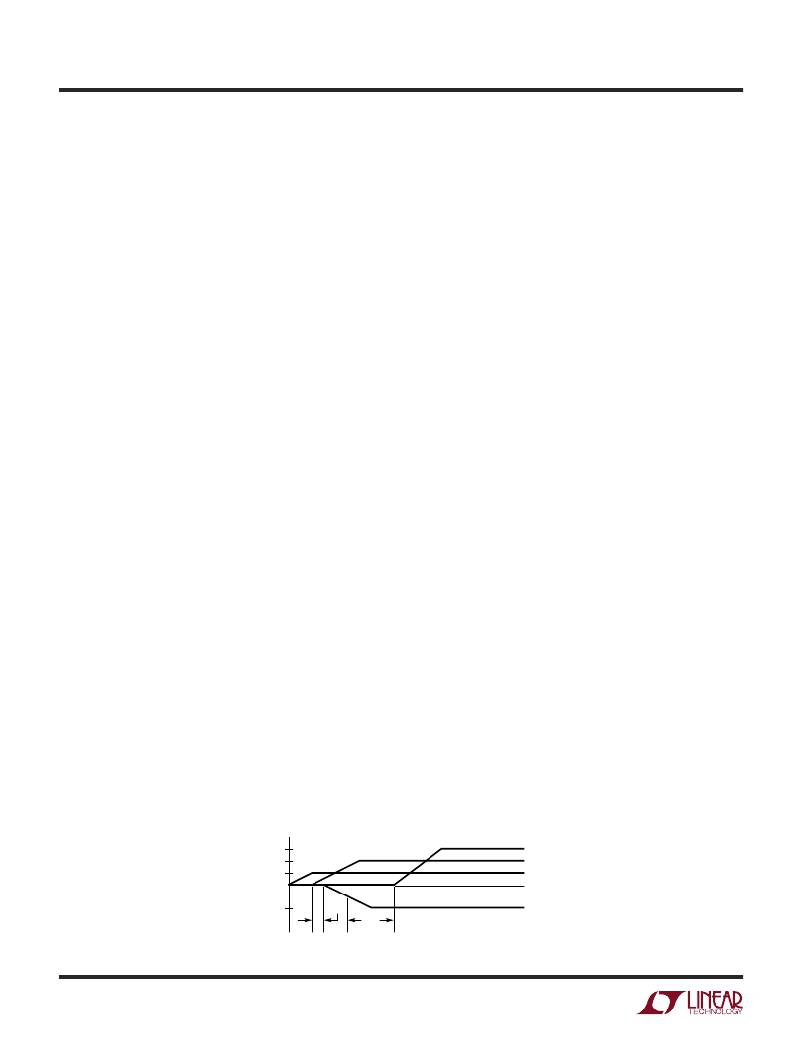
�Output� Sequencing�
�Refer� to� the� following� text� and� Figure� 1� for� the� LTC3450�
�power-up� sequence.� When� input� power� is� applied,� the�
�boost� converter� initializes� and� charges� its� output� towards�
�the� final� value� of� 5.1V.� When� the� boost� converter� output�
�reaches� approximately� 90%� of� its� final� value� (4.5V),� an�
�internal� 5V� OK� signal� is� asserted� which� allows� the� charge�
�pump� doubler� to� begin� operation� toward� its� final� goal� of�
�10V.� Approximately� 1ms� later,� the� charge� pump� inverter�
�begins� operation� toward� its� final� goal� of� either�
�–5V� or� –10V� depending� on� the� connection� of� the� V� INV�
�input.� When� the� –5V� or� –10V� output� (V� NEG� )� reaches�
�approximately� 50%� of� its� final� value,� a� 4ms� (nominal)�
�timeout� period� begins.� At� the� conclusion� of� the� 4ms�
�timeout� period,� the� charge� pump� tripler� is� allowed� to�
�begin� operation,� which� will� eventually� charge� V3X� to� 15V�
�(nominal).�
�15V�
�10V�
�5V�
�–10V�
�V� OUT�
�1ms�
�V� 2X�
�V� NEG�
�V� 3X�
�4ms�
�3450� F01�
�Figure� 1.� Output� Sequencing�
�3450fa�
�8�
�相关PDF资料 |
PDF描述 |
|---|---|
| VE-J5H-EZ-B1 | CONVERTER MOD DC/DC 52V 25W |
| RCB66DHRN-S621 | CONN EDGECARD EXTEND 132POS .050 |
| LT1942EUF#PBF | IC REG SW QUAD TFT LCD 24-QFN |
| MIC37252WU | IC REG LDO ADJ 2.5A TO-263 |
| MIC9131YQS TR | IC CTRLR DC-DC PWM HV HS 16-QSOP |
相关代理商/技术参数 |
参数描述 |
|---|---|
| LTC3450EUD#PBF | 功能描述:IC CONV PS TRIPLE TFT/LCD 16QFN RoHS:是 类别:集成电路 (IC) >> PMIC - 稳压器 - 专用型 系列:- 标准包装:2,000 系列:- 应用:控制器,DSP 输入电压:4.5 V ~ 25 V 输出数:2 输出电压:最低可调至 1.2V 工作温度:-40°C ~ 85°C 安装类型:表面贴装 封装/外壳:30-TFSOP(0.173",4.40mm 宽) 供应商设备封装:30-TSSOP 包装:带卷 (TR) |
| LTC3450EUD#TR | 功能描述:IC CONV PS TRIPLE TFT/LCD 16QFN RoHS:否 类别:集成电路 (IC) >> PMIC - 稳压器 - 专用型 系列:- 标准包装:43 系列:- 应用:控制器,Intel VR11 输入电压:5 V ~ 12 V 输出数:1 输出电压:0.5 V ~ 1.6 V 工作温度:-40°C ~ 85°C 安装类型:表面贴装 封装/外壳:48-VFQFN 裸露焊盘 供应商设备封装:48-QFN(7x7) 包装:管件 |
| LTC3450EUD#TRPBF | 功能描述:IC CONV PS TRIPLE TFT/LCD 16QFN RoHS:是 类别:集成电路 (IC) >> PMIC - 稳压器 - 专用型 系列:- 标准包装:43 系列:- 应用:控制器,Intel VR11 输入电压:5 V ~ 12 V 输出数:1 输出电压:0.5 V ~ 1.6 V 工作温度:-40°C ~ 85°C 安装类型:表面贴装 封装/外壳:48-VFQFN 裸露焊盘 供应商设备封装:48-QFN(7x7) 包装:管件 |
| LTC3452 | 制造商:LINER 制造商全称:Linear Technology 功能描述:Synchronous Buck-Boost MAIN/CAMERA White LED Driver |
| LTC3452EUF | 制造商:LINER 制造商全称:Linear Technology 功能描述:Synchronous Buck-Boost MAIN/CAMERA White LED Driver |
发布紧急采购,3分钟左右您将得到回复。