- 您现在的位置:买卖IC网 > PDF目录1829 > LTC3521IFE#TRPBF (Linear Technology)IC REG BUCK BST SYNC ADJ 20TSSOP PDF资料下载
参数资料
| 型号: | LTC3521IFE#TRPBF |
| 厂商: | Linear Technology |
| 文件页数: | 14/22页 |
| 文件大小: | 0K |
| 描述: | IC REG BUCK BST SYNC ADJ 20TSSOP |
| 标准包装: | 2,500 |
| 类型: | 降压(降压),升压(升压) |
| 输出类型: | 可调式 |
| 输出数: | 3 |
| 输出电压: | 0.6 V ~ 5.5 V,1.8 V ~ 5.25 V |
| 输入电压: | 1.8 V ~ 5.5 V |
| PWM 型: | 电流模式,混合 |
| 频率 - 开关: | 1.1MHz |
| 电流 - 输出: | 600mA,1A |
| 同步整流器: | 是 |
| 工作温度: | -40°C ~ 125°C |
| 安装类型: | 表面贴装 |
| 封装/外壳: | 20-TSSOP(0.173",4.40mm 宽)裸露焊盘 |
| 包装: | 带卷 (TR) |
| 供应商设备封装: | 20-TSSOP-EP |
�� �
�
�LTC3521�
�APPLICATIONS� INFORMATION�
�The� basic� LTC3521� application� circuit� is� shown� as� the�
�Typical� Application� on� the� front� page� of� this� data� sheet.�
�The� external� component� selection� is� determined� by� the�
�desired� output� voltages,� output� currents� and� ripple� volt-�
�age� requirements� of� each� particular� application.� Basic�
�guidelines� and� considerations� for� the� design� process� are�
�provided� in� this� section.�
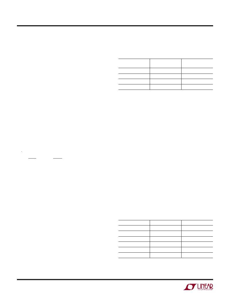
�Table� 1� depicts� the� recommended� inductance� for� several�
�common� output� voltages.�
�Table� 1.� Buck� Recommended� Inductance�
�MINIMUM� MAXIMUM�
�OUTPUT� VOLTAGE� INDUCTANCE� INDUCTANCE�
�0.6V� 1.5μH� 2.2μH�
�1.2V� 2.2μH� 4.7μH�
�Buck� Inductor� Selection�
�1.8V�
�3.3μH�
�6.8μH�
�V� OUT� ?� 1� –� OUT� ?� (� μH� )�
�Thechoiceofbuckinductorvalueinfluencesboththeef-�
�ficiency� and� the� magnitude� of� the� output� voltage� ripple.�
�Larger� inductance� values� will� reduce� inductor� current�
�ripple� and� lead� to� lower� output� voltage� ripple.� For� a� fixed�
�DC� resistance,� a� larger� value� inductor� will� yield� higher�
�efficiency� by� lowering� the� peak� current� closer� to� the� av-�
�erage.� However,� a� larger� inductor� within� the� same� family�
�will� generally� have� a� greater� series� resistance,� thereby�
�offsetting� this� efficiency� advantage.�
�Given� a� desired� peak-to-peak� current� ripple,� ΔI� L� ,� the� required�
�inductance� can� be� calculated� via� the� following� expression,�
�where� f� represents� the� switching� frequency� in� MHz:�
�1� ?� V� ?�
�L� =�
�f� Δ� I� L� ?� V� IN� ?�
�A� reasonable� choice� for� ripple� current� is� ΔI� L� =� 240mA�
�which� represents� 40%� of� the� maximum� 600mA� load�
�current.� The� DC� current� rating� of� the� inductor� should� be�
�at� least� equal� to� the� maximum� load� current,� plus� half� the�
�ripple� current,� in� order� to� prevent� core� saturation� and� loss�
�of� efficiency� during� operation.� To� optimize� efficiency,� the�
�inductor� should� have� a� low� series� resistance.�
�In� particularly� space-restricted� applications,� it� may� be�
�advantageous� to� use� a� much� smaller� value� inductor� at�
�the� expense� of� larger� ripple� current.� In� such� cases,� the�
�converter� will� operate� in� discontinuous� conduction� for� a�
�wider� range� of� output� loads� and� efficiency� will� be� reduced.�
�In� addition,� there� is� a� minimum� inductor� value� required�
�to� maintain� stability� of� the� current� loop� (given� the� fixed�
�internal� slope� compensation).� Specifically,� if� the� buck�
�converter� is� going� to� be� utilized� at� duty� cycles� over� 40%,�
�the� inductance� value� must� be� at� least� L� MIN� ,� as� given� by�
�the� following� equation:�
�L� MIN� =� 2.5� ?� V� OUT� (μH)�
�2.5V� 4.7μH� 8.2μH�
�Buck� Output� Capacitor� Selection�
�A� low� ESR� output� capacitor� should� be� utilized� at� the� buck�
�output� in� order� to� minimize� voltage� ripple.� Multilayer� ce-�
�ramic� capacitors� are� an� excellent� choice� as� they� have� low�
�ESR� and� are� available� in� small� footprints.� In� addition� to�
�controlling� the� ripple� magnitude,� the� value� of� the� output�
�capacitor� also� sets� the� loop� crossover� frequency� and� can,�
�therefore,� impact� loop� stability.� There� is� both� a� minimum�
�and� maximum� capacitance� value� required� to� ensure� stabil-�
�ity� of� the� loop.� If� the� output� capacitance� is� too� small,� the�
�loop� crossover� frequency� will� increase� to� the� point� where�
�the� switching� delay� and� the� high� frequency� parasitic� poles�
�of� the� error� amplifier� will� degrade� the� phase� margin.� In�
�addition,� the� wider� bandwidth� produced� by� a� small� output�
�capacitor� will� make� the� loop� more� susceptible� to� switch-�
�ing� noise.� At� the� other� extreme,� if� the� output� capacitor�
�is� too� large,� the� crossover� frequency� can� decrease� too�
�far� below� the� compensation� zero� and� lead� to� a� degraded�
�phase� margin.� Table� 2� provides� a� guideline� for� the� range�
�of� allowable� values� of� low� ESR� output� capacitors.� Larger�
�value� output� capacitors� can� be� accommodated� provided�
�they� have� sufficient� ESR� to� stabilize� the� loop.�
�Table� 2.� Buck� Output� Capacitor� Range�
�V� OUT� C� MIN� C� MAX�
�0.6V� 15μF� 300μF�
�0.8V� 15μF� 230μF�
�1.2V� 10μF� 150μF�
�1.8V� 10μF� 90μF�
�2.7V� 10μF� 70μF�
�3.3V� 6.8μF� 50μF�
�14�
�For� more� information� www.linear.com/LTC3521�
�3521fb�
�相关PDF资料 |
PDF描述 |
|---|---|
| LTC3522EUD#TRPBF | IC REG BUCK BOOST SYNC ADJ 16QFN |
| LTC3523EUD-2#TRPBF | IC REG BUCK BOOST SYNC ADJ 16QFN |
| LTC3525ESC6-3.3#TRPBF | IC REG BST SYNC 3.3V 0.4A SC70-6 |
| LTC3526BEDC#TRPBF | IC REG BOOST SYNC ADJ 0.5A 6DFN |
| LTC3527EUD-1#TRPBF | IC REG BOOST SYNC ADJ DL 16QFN |
相关代理商/技术参数 |
参数描述 |
|---|---|
| LTC3521IUF#PBF | 功能描述:IC REG BUCK BOOST SYNC ADJ 24QFN RoHS:是 类别:集成电路 (IC) >> PMIC - 稳压器 - DC DC 开关稳压器 系列:- 设计资源:Design Support Tool 标准包装:1 系列:- 类型:升压(升压) 输出类型:固定 输出数:1 输出电压:3V 输入电压:0.75 V ~ 2 V PWM 型:- 频率 - 开关:- 电流 - 输出:100mA 同步整流器:是 工作温度:-40°C ~ 85°C 安装类型:表面贴装 封装/外壳:SOT-23-5 细型,TSOT-23-5 包装:剪切带 (CT) 供应商设备封装:TSOT-23-5 其它名称:AS1323-BTTT-30CT |
| LTC3521IUF#TRPBF | 功能描述:IC REG BUCK BOOST SYNC ADJ 24QFN RoHS:是 类别:集成电路 (IC) >> PMIC - 稳压器 - DC DC 开关稳压器 系列:- 设计资源:Design Support Tool 标准包装:1 系列:- 类型:升压(升压) 输出类型:固定 输出数:1 输出电压:3V 输入电压:0.75 V ~ 2 V PWM 型:- 频率 - 开关:- 电流 - 输出:100mA 同步整流器:是 工作温度:-40°C ~ 85°C 安装类型:表面贴装 封装/外壳:SOT-23-5 细型,TSOT-23-5 包装:剪切带 (CT) 供应商设备封装:TSOT-23-5 其它名称:AS1323-BTTT-30CT |
| LTC3522 | 制造商:LINER 制造商全称:Linear Technology 功能描述:Synchronous 400mA Buck-Boost and 200mA Buck Converters |
| LTC3522EUD | 制造商:LINER 制造商全称:Linear Technology 功能描述:Synchronous 400mA Buck-Boost and 200mA Buck Converters |
| LTC3522EUD#PBF | 功能描述:IC REG BUCK BOOST SYNC ADJ 16QFN RoHS:是 类别:集成电路 (IC) >> PMIC - 稳压器 - DC DC 开关稳压器 系列:- 产品培训模块:MIC23xxx HyperLight Load™ Regulators 标准包装:5,000 系列:HyperLight Load® 类型:降压(降压) 输出类型:固定 输出数:1 输出电压:1.8V 输入电压:2.7 V ~ 5.5 V PWM 型:混合物 频率 - 开关:4MHz 电流 - 输出:2A 同步整流器:是 工作温度:-40°C ~ 125°C 安装类型:表面贴装 封装/外壳:8-VFDFN 裸露焊盘,8-MLF? 包装:带卷 (TR) 供应商设备封装:8-MLF?(2x2) 产品目录页面:1094 (CN2011-ZH PDF) 其它名称:576-3303-2 |
发布紧急采购,3分钟左右您将得到回复。