- 您现在的位置:买卖IC网 > PDF目录1830 > LTC3526BEDC#TRPBF (Linear Technology)IC REG BOOST SYNC ADJ 0.5A 6DFN PDF资料下载
参数资料
| 型号: | LTC3526BEDC#TRPBF |
| 厂商: | Linear Technology |
| 文件页数: | 6/16页 |
| 文件大小: | 0K |
| 描述: | IC REG BOOST SYNC ADJ 0.5A 6DFN |
| 标准包装: | 2,500 |
| 类型: | 升压(升压) |
| 输出类型: | 可调式 |
| 输出数: | 1 |
| 输出电压: | 1.6 V ~ 5.25 V |
| 输入电压: | 0.5 V ~ 5 V |
| PWM 型: | 电流模式,Burst Mode? |
| 频率 - 开关: | 1MHz |
| 电流 - 输出: | 500mA |
| 同步整流器: | 是 |
| 工作温度: | -40°C ~ 85°C |
| 安装类型: | 表面贴装 |
| 封装/外壳: | 6-WFDFN 裸露焊盘 |
| 包装: | 带卷 (TR) |
| 供应商设备封装: | 6-DFN-EP(2x2) |
�� �
�
�LTC3526/LTC3526B�
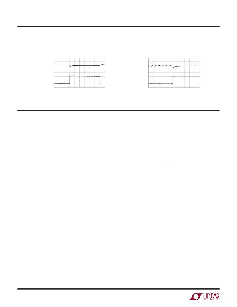
�TYPICAL� PERFORMANCE� CHARACTERISTICS�
�V� OUT�
�100mV/DIV�
�AC-COUPLED�
�LOAD�
�CURRENT�
�50mA/DIV�
�Load� Step� Response�
�(Fixed� Frequency)�
�V� OUT�
�100mV/DIV�
�AC-COUPLED�
�LOAD�
�CURRENT�
�50mA/DIV�
�Load� Step� Response� (from� Burst�
�Mode� Operation)�
�V� IN� =� 1.2V� 100μs/DIV�
�V� OUT� =� 3.3V�
�50mA� TO� 100mA� STEP�
�C� OUT� =� 10μF�
�3526� G21�
�V� IN� =� 1.2V� 50μs/DIV�
�V� OUT� =� 3.3V�
�5mA� TO� 100mA� STEP�
�C� OUT� =� 10μF�
�3526� G22�
�ELECTRICAL� CHARACTERISTICS�
�SW� (Pin� 1):� Switch� Pin.� Connect� inductor� between� SW� and�
�V� IN� .� Keep� PCB� trace� lengths� as� short� and� wide� as� possible�
�to� reduce� EMI.� If� the� inductor� current� falls� to� zero� or� SHDN�
�is� low,� an� internal� anti-ringing� switch� is� connected� from�
�SW� to� V� IN� to� minimize� EMI.�
�FB� (Pin� 5):� Feedback� Input� to� the� g� m� Error� Amplifier.� Con-�
�nect� resistor� divider� tap� to� this� pin.� The� top� of� the� divider�
�connects� to� the� output� capacitor,� the� bottom� of� the� divider�
�connects� to� GND.� Referring� to� the� Block� Diagram,� the� output�
�voltage� can� be� adjusted� from� 1.6V� to� 5.25V� by:�
�V� OUT� =� 1� .� 195� V� ?� ?� 1� +�
�GND(Pin2):� SignalandPowerGround.Provideashort�
�direct� PCB� path� between� GND� and� the� (–)� side� of� the� input�
�and� output� capacitors.�
�?�
�?�
�R2� ?�
�R� 1� ?� ?�
�V� IN� (Pin� 3):� Input� Supply� Pin.� Connect� a� minimum� of� 1μF�
�ceramic� decoupling� capacitor� from� this� pin� to� ground�
�using� short� direct� PCB� traces.�
�SHDN� (Pin� 4):� Logic� Controlled� Shutdown� Input.� There�
�is� an� internal� 4M� Ω� pull-down� on� this� pin.�
�?� SHDN� =� High:� Normal� operation�
�?� SHDN� =� Low:� Shutdown,� quiescent� current� <� 1μA�
�V� OUT� (Pin� 6):� Output� voltage� sense� and� drain� of� the� internal�
�synchronous� rectifier.� PCB� trace� from� V� OUT� to� the� output�
�filter� capacitor� (4.7μF� minimum)� should� be� as� short� and�
�wide� as� possible.�
�GND� (Exposed� Pad� Pin� 7):� The� Exposed� Pad� must� be� sol-�
�dered� to� the� PCB� ground� plane.� It� serves� as� an� additional�
�ground� connection� and� as� a� means� of� conducting� heat�
�away� from� the� package.�
�3526bfd�
� �
�相关PDF资料 |
PDF描述 |
|---|---|
| LTC3527EUD-1#TRPBF | IC REG BOOST SYNC ADJ DL 16QFN |
| LTC3528EDDB#TRPBF | IC REG BOOST SYNC ADJ 1A 8DFN |
| LTC3529EDCB#TRPBF | IC REG BOOST SYNC 5V 1.5A 8DFN |
| LTC3530EMS#TRPBF | IC REG BUCK BST SYNC 0.6A 10MSOP |
| LTC3531ES6-3.3#TRPBF | IC REG BUCK BST SYNC 3.3V TSOT23 |
相关代理商/技术参数 |
参数描述 |
|---|---|
| LTC3526EDC | 制造商:LINER 制造商全称:Linear Technology 功能描述:500mA 1MHz Synchronous Step-Up DC/DC Converters in 2mm X 2mm DFN |
| LTC3526EDC#PBF | 制造商:Linear Technology 功能描述:IC SYNC STEP-UP DC/DC CONVERTER DFN-6 制造商:Linear Technology 功能描述:IC, SYNC STEP-UP DC/DC CONVERTER, DFN-6 制造商:Linear Technology 功能描述:IC, SYNC STEP-UP DC/DC CONVERTER, DFN-6; Primary Input Voltage:6V; No. of Outputs:1; Output Voltage:5.25V; Output Current:500mA; No. of Pins:6; Operating Temperature Min:-40C; Operating Temperature Max:85C; MSL:MSL 1 - Unlimited ;RoHS Compliant: Yes |
| LTC3526EDC#TRMPBF | 功能描述:IC REG BOOST SYNC ADJ 0.5A 6DFN RoHS:是 类别:集成电路 (IC) >> PMIC - 稳压器 - DC DC 开关稳压器 系列:- 标准包装:2,500 系列:- 类型:升压(升压) 输出类型:可调式 输出数:1 输出电压:1.24 V ~ 30 V 输入电压:1.5 V ~ 12 V PWM 型:电流模式,混合 频率 - 开关:600kHz 电流 - 输出:500mA 同步整流器:无 工作温度:-40°C ~ 85°C 安装类型:表面贴装 封装/外壳:8-SOIC(0.154",3.90mm 宽) 包装:带卷 (TR) 供应商设备封装:8-SOIC |
| LTC3526EDC#TRPBF | 功能描述:IC REG BOOST SYNC ADJ 0.5A 6DFN RoHS:是 类别:集成电路 (IC) >> PMIC - 稳压器 - DC DC 开关稳压器 系列:- 标准包装:2,500 系列:- 类型:升压(升压) 输出类型:可调式 输出数:1 输出电压:1.24 V ~ 30 V 输入电压:1.5 V ~ 12 V PWM 型:电流模式,混合 频率 - 开关:600kHz 电流 - 输出:500mA 同步整流器:无 工作温度:-40°C ~ 85°C 安装类型:表面贴装 封装/外壳:8-SOIC(0.154",3.90mm 宽) 包装:带卷 (TR) 供应商设备封装:8-SOIC |
| LTC3526EDC-2#TRMPBF | 功能描述:IC REG BOOST SYNC ADJ 0.5A 6DFN RoHS:是 类别:集成电路 (IC) >> PMIC - 稳压器 - DC DC 开关稳压器 系列:- 标准包装:2,500 系列:- 类型:升压(升压) 输出类型:可调式 输出数:1 输出电压:1.24 V ~ 30 V 输入电压:1.5 V ~ 12 V PWM 型:电流模式,混合 频率 - 开关:600kHz 电流 - 输出:500mA 同步整流器:无 工作温度:-40°C ~ 85°C 安装类型:表面贴装 封装/外壳:8-SOIC(0.154",3.90mm 宽) 包装:带卷 (TR) 供应商设备封装:8-SOIC |
发布紧急采购,3分钟左右您将得到回复。