- 您现在的位置:买卖IC网 > PDF目录14013 > LTC3527EUD-1#PBF (Linear Technology)IC REG BOOST SYNC ADJ DL 16QFN PDF资料下载
参数资料
| 型号: | LTC3527EUD-1#PBF |
| 厂商: | Linear Technology |
| 文件页数: | 13/22页 |
| 文件大小: | 0K |
| 描述: | IC REG BOOST SYNC ADJ DL 16QFN |
| 标准包装: | 121 |
| 类型: | 升压(升压) |
| 输出类型: | 可调式 |
| 输出数: | 2 |
| 输出电压: | 1.6 V ~ 5.25 V |
| 输入电压: | 0.5 V ~ 5 V |
| PWM 型: | 电流模式,混合 |
| 频率 - 开关: | 1.2MHz,2.2MHz |
| 电流 - 输出: | 400mA,800mA |
| 同步整流器: | 是 |
| 工作温度: | -40°C ~ 85°C |
| 安装类型: | 表面贴装 |
| 封装/外壳: | 16-WFQFN 裸露焊盘 |
| 包装: | 管件 |
| 供应商设备封装: | 16-QFN(3x3) |
�� �
�
�LTC3527/LTC3527-1�
�APPLICATIONS� INFORMATION�
�PCB� Layout� Guidelines�
�The� minimum� inductance� value� is� given� by:�
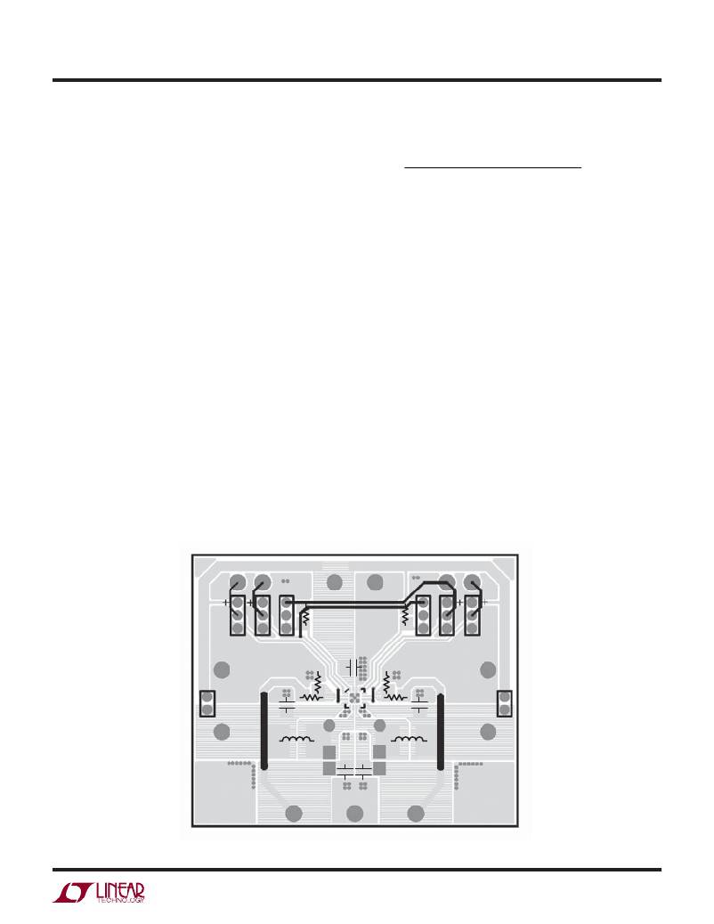
�The� high� speed� operation� of� the� LTC3527/LTC3527-1�
�demands� careful� attention� to� board� layout.� A� careless�
�layout� will� result� in� reduced� performance.� Figure� 1� shows�
�L� >�
�V� IN(MIN)� ? ( V� OUT(MAX )� – V� IN(MIN)� )�
�f� ?� Ripple� ?� V� OU� T� (� MAX� )�
�the� recommended� component� placement.� A� large� ground�
�pin� copper� area� will� help� to� lower� the� die� temperature.� A�
�multilayer� board� with� a� separate� ground� plane� is� ideal,� but�
�not� absolutely� necessary.�
�COMPONENT� SELECTION�
�Inductor� Selection�
�The� LTC3527/LTC3527-1� can� utilize� small� surface� mount�
�inductors� due� to� their� fast� 1.2MHz/2.2MHz� switching�
�frequencies.� Inductor� values� between� 3.3μH� and� 4.7μH�
�are� suitable� for� most� 1.2MHz� applications.� Inductor� values�
�between� 1.5μH� and� 2.2μH� are� suitable� for� most� 2.2MHz�
�applications.� Larger� values� of� inductance� will� allow� slightly�
�greater� output� current� capability� (and� lower� the� Burst�
�Mode� threshold)� by� reducing� the� inductor� ripple� cur-�
�rent.� Increasing� the� inductance� above� 10μH� will� increase�
�size� while� providing� little� improvement� in� output� current�
�capability.�
�where:�
�Ripple� =� Allowable� inductor� current� ripple� (amps�
�peak-to-peak)�
�V� IN(MIN)� =� Minimum� input� voltage�
�V� OUT(MAX)� =� Maximum� output� voltage�
�f� =� Oscillator� frequency� (MHz)�
�The� inductor� current� ripple� is� typically� set� for� 20%� to�
�40%� of� the� maximum� inductor� current.� High� frequency�
�ferrite� core� inductor� materials� reduce� frequency� dependent�
�power� losses� compared� to� cheaper� powdered� iron� types,�
�improving� ef?ciency.� The� inductor� should� have� low� ESR�
�(series� resistance� of� the� windings)� to� reduce� the� I� 2� R� power�
�losses,� and� must� be� able� to� support� the� peak� inductor�
�current� without� saturating.� Molded� chokes� and� some�
�chip� inductors� usually� do� not� have� enough� core� area� to�
�support� the� peak� inductor� currents� of� 900mA� (500mA)�
�seen� on� the� LTC3527/LTC3527-1.� To� minimize� radiated�
�noise,� use� shielded� inductors.� See� Table� 1� for� suggested�
�components� and� suppliers.�
�MODE� SHDN1�
�GND�
�V� IN1�
�V� OUT1�
�V� IN�
�GND�
�GND�
�V� OUT2�
�SHDN2� FSEL�
�GND�
�V� IN2�
�35271� F01�
�Figure� 1.� Recommended� Component� Placement� for� a� Dual-Layer� Board�
�35271fc�
�13�
�相关PDF资料 |
PDF描述 |
|---|---|
| V28C24C100BF3 | CONVERTER MOD DC/DC 24V 100W |
| LTC3527EUD#PBF | IC REG BOOST SYNC ADJ DL 16QFN |
| MAX6717AUKZWD6+T | IC SUPERVISOR MPU SOT23-5 |
| MAX6717AUKZWD2+T | IC SUPERVISOR MPU SOT23-5 |
| LT3663IDCB#TRPBF | IC REG BUCK ADJ 1.2A 8DFN |
相关代理商/技术参数 |
参数描述 |
|---|---|
| LTC3527EUD-1-TR | 制造商:LINER 制造商全称:Linear Technology 功能描述:Dual 800mA/400mA, 1.2MHz/2.2MHz Synchronous Step-Up DC/DC Converters |
| LTC3527EUD-1-TRPBF | 制造商:LINER 制造商全称:Linear Technology 功能描述:Dual 800mA/400mA, 1.2MHz/2.2MHz Synchronous Step-Up DC/DC Converters |
| LTC3527EUD-PBF | 制造商:LINER 制造商全称:Linear Technology 功能描述:Dual 800mA/400mA, 1.2MHz/2.2MHz Synchronous Step-Up DC/DC Converters |
| LTC3527EUD-TR | 制造商:LINER 制造商全称:Linear Technology 功能描述:Dual 800mA/400mA, 1.2MHz/2.2MHz Synchronous Step-Up DC/DC Converters |
| LTC3527EUD-TRPBF | 制造商:LINER 制造商全称:Linear Technology 功能描述:Dual 800mA/400mA, 1.2MHz/2.2MHz Synchronous Step-Up DC/DC Converters |
发布紧急采购,3分钟左右您将得到回复。