- 您现在的位置:买卖IC网 > PDF目录14013 > LTC3527EUD-1#PBF (Linear Technology)IC REG BOOST SYNC ADJ DL 16QFN PDF资料下载
参数资料
| 型号: | LTC3527EUD-1#PBF |
| 厂商: | Linear Technology |
| 文件页数: | 3/22页 |
| 文件大小: | 0K |
| 描述: | IC REG BOOST SYNC ADJ DL 16QFN |
| 标准包装: | 121 |
| 类型: | 升压(升压) |
| 输出类型: | 可调式 |
| 输出数: | 2 |
| 输出电压: | 1.6 V ~ 5.25 V |
| 输入电压: | 0.5 V ~ 5 V |
| PWM 型: | 电流模式,混合 |
| 频率 - 开关: | 1.2MHz,2.2MHz |
| 电流 - 输出: | 400mA,800mA |
| 同步整流器: | 是 |
| 工作温度: | -40°C ~ 85°C |
| 安装类型: | 表面贴装 |
| 封装/外壳: | 16-WFQFN 裸露焊盘 |
| 包装: | 管件 |
| 供应商设备封装: | 16-QFN(3x3) |
�� �
�
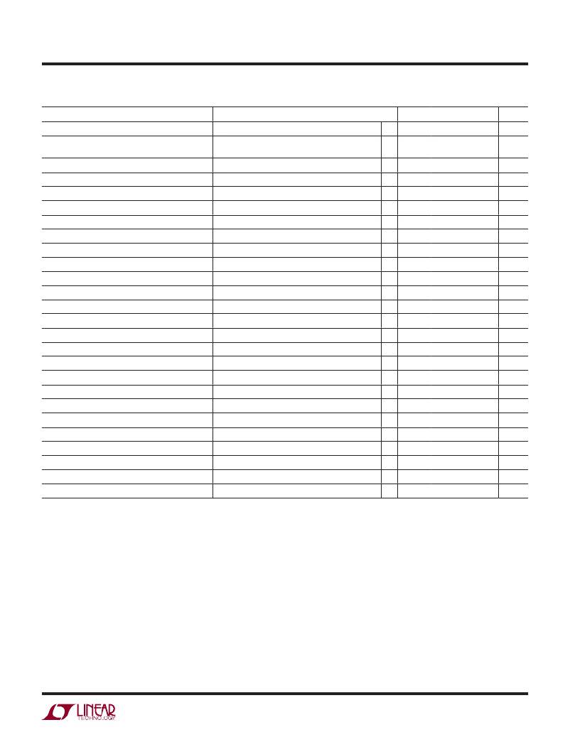
�LTC3527/LTC3527-1�
�ELECTRICAL� CHARACTERISTICS� The� l� denotes� the� speci?cations� which� apply� over� the� full� operating�
�temperature� range,� –40� °� C� to� 85� °� C.� V� IN� =� V� IN1� =� V� IN2� =� 1.2V,� V� OUT1� =� V� OUT2� =� 3.3V,� T� A� =� 25°C,� unless� otherwise� noted.�
�PARAMETER�
�PMOS� Switch� Leakage� Current� (LTC3527)�
�CONDITIONS�
�V� SW1,2� =� 5V,� V� OUT1,2� =� 0V,� SHDN1,2� =� 0V�
�MIN�
�TYP�
�0.1�
�MAX�
�10�
�UNITS�
�μA�
�NMOS� and� PMOS� Combined� Switch� Leakage� Current� V� SW1,2� =� 5V,� V� OUT1,2� =� 0V,� SHDN1,2� =� 0V� (Note� 6)�
�0.2�
�20�
�μA�
�(LTC3527-1)�
�NMOS� Switch� On-Resistance,� SW1�
�NMOS� Switch� On-Resistance,� SW2�
�PMOS� Switch� On-Resistance,� SW1�
�PMOS� Switch� On-Resistance,� SW2�
�0.30�
�0.50�
�0.40�
�0.60�
�Ω�
�Ω�
�Ω�
�Ω�
�NMOS� Current� Limit,� SW1�
�NMOS� Current� Limit,� SW2�
�Current� Limit� Delay� to� Output� Time�
�(Note� 4)�
�l�
�l�
�800�
�400�
�60�
�mA�
�mA�
�ns�
�Maximum� Duty� Cycle�
�Minimum� Duty� Cycle�
�V� FB1,2� =� 1V�
�V� FB1,2� =� 1.3V�
�l�
�l�
�85�
�90�
�0�
�%�
�%�
�Switching� Frequency�
�Switching� Frequency�
�V� FSEL� =� 0V�
�V� FSEL� =� 3.3V�
�l�
�l�
�0.9�
�1.8�
�1.2�
�2.2�
�1.5�
�2.8�
�MHz�
�MHz�
�SHDN1,2� Input� High� Voltage�
�SHDN1,2� Input� Low� Voltage�
�0.88�
�0.35�
�V�
�V�
�SHDN1,2� Input� Current�
�V� SHDN1,2� =� 3.3V�
�1�
�2�
�μA�
�PGOOD1,� PGOOD2� Threshold�
�PGOOD1,� PGOOD2� Low� Voltage�
�PGOOD1,� PGOOD2� Leakage� Current�
�Referenced� to� the� Feedback� Voltage�
�I� PGOOD1,2� =� 1mA�
�V� PGOOD1,2� =� 5.25V�
�–6�
�–9�
�0.1�
�0.01�
�–14�
�0.2�
�1�
�%�
�V�
�μA�
�MODE� Input� High� Voltage�
�MODE� Input� Low� Voltage�
�1�
�0.35�
�V�
�V�
�MODE� Input� Current�
�V� MODE� =� 3.3V�
�1�
�2�
�μA�
�FSEL� Input� High� Voltage�
�FSEL� Input� Low� Voltage�
�0.88�
�0.35�
�V�
�V�
�FSEL� Input� Current�
�Soft-Start� Time�
�V� FSEL� =� 3.3V�
�1�
�0.5�
�2�
�μA�
�ms�
�Note� 1:� Stresses� beyond� those� listed� under� Absolute� Maximum� Ratings�
�may� cause� permanent� damage� to� the� device.� Exposure� to� any� Absolute�
�Maximum� Rating� condition� for� extended� periods� may� affect� device�
�reliability� and� lifetime.�
�Note� 2:� The� LTC3527E/LTC3527E-1� are� guaranteed� to� meet� performance�
�speci?cations� from� 0°C� to� 85°C.� Speci?cations� over� the� –40°C� to� 85°C�
�operating� temperature� range� are� assured� by� design,� characterization� and�
�correlation� with� statistical� process� controls.�
�Note� 3:� Current� is� measured� into� the� V� OUT� pin� since� the� supply� current� is�
�bootstrapped� to� the� output.� The� current� will� re?ect� to� the� input� supply� by:�
�Note� 4:� Speci?cation� is� guaranteed� by� design� and� not� 100%� tested� in�
�production.�
�Note� 5:� The� LTC3527/LTC3527-1� includes� an� overtemperature� shutdown�
�that� is� intended� to� protect� the� device� during� momentary� overload�
�conditions.� Junction� temperature� will� exceed� 125°C� when� the� over-�
�temperature� shutdown� is� active.� Continuous� operation� above� the� speci?ed�
�maximum� junction� temperature� may� impair� device� reliability.�
�Note� 6:� The� NMOS� and� PMOS� switch� leakage� currents� are� tested� in� parallel�
�for� the� LTC3527-1� because� V� OUT1,2� are� actively� pulled� to� ground� when�
�SHDN1,2� =� 0V�
�(V� OUT� /V� IN� )� ?� (1/Ef?ciency).� All� switches� are� off.�
�35271fc�
�3�
�相关PDF资料 |
PDF描述 |
|---|---|
| V28C24C100BF3 | CONVERTER MOD DC/DC 24V 100W |
| LTC3527EUD#PBF | IC REG BOOST SYNC ADJ DL 16QFN |
| MAX6717AUKZWD6+T | IC SUPERVISOR MPU SOT23-5 |
| MAX6717AUKZWD2+T | IC SUPERVISOR MPU SOT23-5 |
| LT3663IDCB#TRPBF | IC REG BUCK ADJ 1.2A 8DFN |
相关代理商/技术参数 |
参数描述 |
|---|---|
| LTC3527EUD-1-TR | 制造商:LINER 制造商全称:Linear Technology 功能描述:Dual 800mA/400mA, 1.2MHz/2.2MHz Synchronous Step-Up DC/DC Converters |
| LTC3527EUD-1-TRPBF | 制造商:LINER 制造商全称:Linear Technology 功能描述:Dual 800mA/400mA, 1.2MHz/2.2MHz Synchronous Step-Up DC/DC Converters |
| LTC3527EUD-PBF | 制造商:LINER 制造商全称:Linear Technology 功能描述:Dual 800mA/400mA, 1.2MHz/2.2MHz Synchronous Step-Up DC/DC Converters |
| LTC3527EUD-TR | 制造商:LINER 制造商全称:Linear Technology 功能描述:Dual 800mA/400mA, 1.2MHz/2.2MHz Synchronous Step-Up DC/DC Converters |
| LTC3527EUD-TRPBF | 制造商:LINER 制造商全称:Linear Technology 功能描述:Dual 800mA/400mA, 1.2MHz/2.2MHz Synchronous Step-Up DC/DC Converters |
发布紧急采购,3分钟左右您将得到回复。