- 您现在的位置:买卖IC网 > PDF目录1830 > LTC3533EDE#TRPBF (Linear Technology)IC REG BUCK BOOST SYNC ADJ 14DFN PDF资料下载
参数资料
| 型号: | LTC3533EDE#TRPBF |
| 厂商: | Linear Technology |
| 文件页数: | 8/16页 |
| 文件大小: | 0K |
| 描述: | IC REG BUCK BOOST SYNC ADJ 14DFN |
| 标准包装: | 2,500 |
| 类型: | 降压(降压),升压(升压) |
| 输出类型: | 可调式 |
| 输出数: | 1 |
| 输出电压: | 1.8 V ~ 5.25 V |
| 输入电压: | 1.8 V ~ 5.5 V |
| PWM 型: | Burst Mode? |
| 频率 - 开关: | 300kHz ~ 2MHz |
| 电流 - 输出: | 2A |
| 同步整流器: | 是 |
| 工作温度: | -40°C ~ 85°C |
| 安装类型: | 表面贴装 |
| 封装/外壳: | 14-WFDFN 裸露焊盘 |
| 包装: | 带卷 (TR) |
| 供应商设备封装: | 14-DFN-EP(4x3) |
�� �
�
�LTC3533�
�OPERATION�
�Error� Ampli?er�
�The� error� ampli?er� is� a� voltage� mode� ampli?er.� The� loop�
�compensation� components� are� con?gured� around� the�
�ampli?er� (from� FB� to� V� C� )� to� obtain� stability� of� the� converter.�
�For� improved� bandwidth,� an� additional� RC� feed-forward�
�network� can� be� placed� across� the� upper� feedback� divider�
�resistor.� The� voltage� on� the� RUN/SS� pin� clamps� the� error�
�ampli?er� output,� V� C� ,� to� provide� a� soft-start� function.�
�Supply� Current� Limits�
�There� are� two� different� supply� current� limit� circuits� in� the�
�LTC3533,� working� consecutively,� each� having� internally�
�?xed� thresholds� which� vary� inversely� with� V� IN� .�
�The� ?rst� circuit� is� a� current� limit� ampli?er,� sourcing� cur-�
�rent� into� FB� to� drop� the� output� voltage,� should� the� peak�
�input� current� exceed� 4.5A� typical.� This� method� provides� a�
�closed� loop� means� of� clamping� the� input� current.� During�
�conditions� where� V� OUT� is� near� ground,� such� as� during� a�
�short� circuit� or� startup,� this� threshold� is� cut� to� 750mA,�
�providing� a� fold-back� feature.� For� this� current� limit� feature�
�to� be� most� effective,� the� Thevenin� resistance� from� FB� to�
�ground� should� be� greater� than� 100k.�
�Should� the� peak� input� current� exceed� 7A� typical,� the� second�
�circuit,� a� high� speed� peak� current� limit� comparator,� shuts�
�off� PMOS� switch� A.� The� delay� to� output� of� this� comparator�
�is� typically� 50ns.�
�Reverse� Current� Limit�
�During� ?xed� frequency� operation,� the� LTC3533� operates� in�
�forced� continuous� conduction� mode.� The� reverse� current�
�output� through� switch� D.� Should� this� negative� inductor�
�current� exceed� 500mA� typical,� the� LTC3533� shuts� off�
�switch� D.�
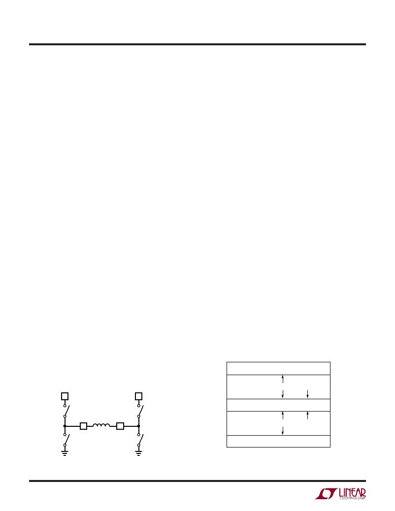
�Four-Switch� Control�
�Figure� 1� shows� a� simpli?ed� diagram� of� how� the� four� in-�
�ternal� switches� are� connected� to� the� inductor,� V� IN� ,� V� OUT�
�and� GND.Figure� 2� shows� the� regions� of� operation� for� the�
�LTC3533� as� a� function� of� the� control� voltage,� V� C� .�
�Dependent� on� V� C� ’s� magnitude,� the� LTC3533� will� operate�
�in� either� buck,� buck/boost� or� boost� mode.� The� four� power�
�switches� are� properly� phased� so� the� transfer� between� op-�
�erating� modes� is� continuous,� smooth� and� transparent� to�
�the� user.� When� V� IN� approaches� V� OUT� the� buck/boost� region�
�is� entered,� where� the� conduction� time� of� the� four� switch�
�region� is� typically� 150ns.� Referring� to� Figures� 1� and� 2,� the�
�various� regions� of� operation� will� now� be� described.�
�Buck� Region� (V� IN� >� V� OUT� )�
�Switch� D� is� always� on� and� switch� C� is� always� off� during�
�this� mode.� When� the� control� voltage,� V� C� ,� is� above� volt-�
�age� V1,� switch� A� begins� to� switch.� During� the� off� time� of�
�switch� A,� synchronous� switch� B� turns� on� for� the� remainder�
�of� the� period.� Switches� A� and� B� will� alternate� similar� to� a�
�typical� synchronous� buck� regulator.� As� the� control� volt-�
�age� increases,� the� duty� cycle� of� switch� A� increases� until�
�the� maximum� duty� cycle� of� the� converter� in� buck� mode�
�reaches� D� MAX_BUCK� ,� given� by:�
�D� MAX_BUCK� =� 100� –� D4� SW� %�
�where� D4� SW� =� duty� cycle� %� of� the� four� switch� range.�
�limit� comparator� monitors� the� inductor� current� from� the�
�85%�
�D� MAX�
�BOOST�
�V4� (� ≈� 1.5V)�
�PV� IN�
�11�
�PV� OUT�
�9�
�D� MIN�
�BOOST�
�A� ON,� B� OFF�
�PWM� CD� SWITCHES�
�BOOST� REGION�
�V3� (� ≈� 1.15V)�
�PMOS� A�
�PMOS� D�
�D� MAX�
�BUCK�
�FOUR� SWITCH� PWM�
�BUCK/BOOST� REGION�
�V2� (� ≈� 1V)�
�SW1�
�3�
�L1�
�SW2�
�7�
�D� ON,� C� OFF�
�PWM� AB� SWITCHES� BUCK� REGION�
�NMOS� B�
�NMOS� C�
�0%�
�DUTY�
�V1� (� ≈� 0.7V)�
�CONTROL�
�3533� F01�
�CYCLE�
�3533� F02�
�VOLTAGE,� V� C�
�Figure� 1.� Simpli?ed� Diagram� of� Output� Switches�
�Figure� 2.� Switch� Control� vs� Control� Voltage,� V� C�
�3533f�
�8�
�相关PDF资料 |
PDF描述 |
|---|---|
| LTC3534EGN#TRPBF | IC REG BUCK BST SYNC 0.5A 16SSOP |
| LTC3535EDD#PBF | IC REG BST SYNC ADJ 0.55A 12DFN |
| LTC3536IMSE#TRPBF | IC REG BUCK BST SYNC ADJ 12MSOP |
| LTC3538EDCB#TRPBF | IC REG BUCK BOOST SYNC ADJ 8DFN |
| LTC3539EDCB-2#TRPBF | IC REG BOOST SYNC ADJ 2A 8DFN |
相关代理商/技术参数 |
参数描述 |
|---|---|
| LTC3534 | 制造商:LINER 制造商全称:Linear Technology 功能描述:40V, 2A Synchronous Buck-Boost DC/DC |
| LTC3534EDHC#PBF | 功能描述:IC REG BUCK BOOST SYNC ADJ 16DFN RoHS:是 类别:集成电路 (IC) >> PMIC - 稳压器 - DC DC 开关稳压器 系列:- 标准包装:2,500 系列:- 类型:降压(降压) 输出类型:固定 输出数:1 输出电压:1.2V,1.5V,1.8V,2.5V 输入电压:2.7 V ~ 20 V PWM 型:- 频率 - 开关:- 电流 - 输出:50mA 同步整流器:是 工作温度:-40°C ~ 125°C 安装类型:表面贴装 封装/外壳:10-TFSOP,10-MSOP(0.118",3.00mm 宽)裸露焊盘 包装:带卷 (TR) 供应商设备封装:10-MSOP 裸露焊盘 |
| LTC3534EDHC#TRPBF | 功能描述:IC REG BUCK BOOST SYNC ADJ 16DFN RoHS:是 类别:集成电路 (IC) >> PMIC - 稳压器 - DC DC 开关稳压器 系列:- 标准包装:2,500 系列:- 类型:降压(降压) 输出类型:固定 输出数:1 输出电压:1.2V,1.5V,1.8V,2.5V 输入电压:2.7 V ~ 20 V PWM 型:- 频率 - 开关:- 电流 - 输出:50mA 同步整流器:是 工作温度:-40°C ~ 125°C 安装类型:表面贴装 封装/外壳:10-TFSOP,10-MSOP(0.118",3.00mm 宽)裸露焊盘 包装:带卷 (TR) 供应商设备封装:10-MSOP 裸露焊盘 |
| LTC3534EGN#PBF | 功能描述:IC REG BUCK BST SYNC 0.5A 16SSOP RoHS:是 类别:集成电路 (IC) >> PMIC - 稳压器 - DC DC 开关稳压器 系列:- 标准包装:250 系列:- 类型:降压(降压) 输出类型:固定 输出数:1 输出电压:1.2V 输入电压:2.05 V ~ 6 V PWM 型:电压模式 频率 - 开关:2MHz 电流 - 输出:500mA 同步整流器:是 工作温度:-40°C ~ 85°C 安装类型:表面贴装 封装/外壳:6-UFDFN 包装:带卷 (TR) 供应商设备封装:6-SON(1.45x1) 产品目录页面:1032 (CN2011-ZH PDF) 其它名称:296-25628-2 |
| LTC3534EGN#TRPBF | 功能描述:IC REG BUCK BST SYNC 0.5A 16SSOP RoHS:是 类别:集成电路 (IC) >> PMIC - 稳压器 - DC DC 开关稳压器 系列:- 标准包装:2,500 系列:- 类型:降压(降压) 输出类型:固定 输出数:1 输出电压:1.2V,1.5V,1.8V,2.5V 输入电压:2.7 V ~ 20 V PWM 型:- 频率 - 开关:- 电流 - 输出:50mA 同步整流器:是 工作温度:-40°C ~ 125°C 安装类型:表面贴装 封装/外壳:10-TFSOP,10-MSOP(0.118",3.00mm 宽)裸露焊盘 包装:带卷 (TR) 供应商设备封装:10-MSOP 裸露焊盘 |
发布紧急采购,3分钟左右您将得到回复。