- 您现在的位置:买卖IC网 > PDF目录13970 > LTC3536IMSE#PBF (Linear Technology)IC REG BUCK BST SYNC ADJ 12MSOP PDF资料下载
参数资料
| 型号: | LTC3536IMSE#PBF |
| 厂商: | Linear Technology |
| 文件页数: | 10/28页 |
| 文件大小: | 0K |
| 描述: | IC REG BUCK BST SYNC ADJ 12MSOP |
| 标准包装: | 37 |
| 类型: | 降压(降压),升压(升压) |
| 输出类型: | 可调式 |
| 输出数: | 1 |
| 输出电压: | 1.8 V ~ 5.5 V |
| 输入电压: | 1.8 V ~ 5.5 V |
| PWM 型: | 电压模式,混合 |
| 频率 - 开关: | 300kHz ~ 2MHz |
| 电流 - 输出: | 1A |
| 同步整流器: | 是 |
| 工作温度: | -40°C ~ 125°C |
| 安装类型: | 表面贴装 |
| 封装/外壳: | 12-TSSOP (0.118",3.00mm 宽)裸露焊盘 |
| 包装: | 管件 |
| 供应商设备封装: | 12-MSOP,裸露焊盘 |
第1页第2页第3页第4页第5页第6页第7页第8页第9页当前第10页第11页第12页第13页第14页第15页第16页第17页第18页第19页第20页第21页第22页第23页第24页第25页第26页第27页第28页
�� �
�
�LTC3536�
�OPERATION�
�R� TOP� 0.6V� +�
�C� FF�
�–�
�R� FB�
�diode from the RT pin to V� IN� can be used in addition to�
�current� limiting� resistor.� For� noise� sensitive� applications,�
�an� internal� phase-locked� loop� allows� the� LTC3536� to�
�be� synchronized� to� an� external� clock� signal� applied� to�
�the� MODE/SYNC� pin.� The� free-running� frequency� of� the�
�oscillator� can� be� programmed� slower� or� faster� than� the�
�synchronization� clock� frequency.�
�Whether� operating� from� its� internal� oscillator� or� when�
�synchronized� to� an� external� clock� signal,� the� LTC3536� is�
�able� to� operate� with� a� switching� frequency� from� 300kHz�
�to� 2MHz,� providing� the� ability� to� minimize� the� size� of� the�
�external� components� and� optimize� the� power� conversion�
�efficiency.�
�Error� Amplifier�
�The� LTC3536� has� an� internal� high� gain� operational� ampli-�
�fier� which� provides� frequency� compensation� of� the� control�
�loop� that� maintains� output� voltage� regulation.� To� ensure�
�stability� of� this� control� loop,� an� external� compensation�
�network� must� be� installed� in� the� application� circuit.� A�
�Type� III� compensation� network� as� shown� in� Figure� 2� is�
�recommended� for� most� applications� since� it� provides� the�
�flexibility� to� optimize� the� converter’s� transient� response�
�while� simultaneously� minimizing� any� DC� error� in� the� output�
�voltage.� Details� on� designing� the� compensation� network�
�in� LTC3536� applications� can� be� found� in� the� Applications�
�Information� section� of� this� data� sheet.�
�V� OUT�
�R� FF� LTC3536�
�FB� PWM�
�C� FB�
�R� BOT� VC�
�GND�
�C� POLE� 3536� F02�
�Figure� 2.� Error� Amplifier� and� Compensation� Network�
�Input� and� Peak� Current� Limits�
�The� LTC3536� has� two� current� limit� circuits� that� are� de-�
�signed� to� limit� the� peak� inductor� current� to� ensure� that�
�the� switch� currents� remain� within� the� capabilities� of� the�
�IC� during� output� short-circuit� or� overload� conditions.� The�
�input� current� limit� operates� by� injecting� a� current� into� the�
�feedback� pin,� which� is� proportional� to� the� extent� that� the�
�inductor� current� exceeds� the� input� current� limit� threshold�
�(typically� 2.5A).� Due� to� the� high� gain� of� the� feedback� loop,�
�this� injected� current� forces� the� error� amplifier� output� to�
�decrease� until� the� average� current� through� the� inductor�
�is� approximately� reduced� to� the� current� limit� threshold.�
�For� this� current� limit� feature� to� be� most� effective,� the�
�Thevenin� resistance� (R� BOT� //R� TOP� )� from� FB� to� ground�
�should� exceed� 100kΩ.�
�15�
�14�
�13�
�12�
�11�
�10�
�9�
�8�
�7�
�6�
�5�
�4�
�3�
�2�
�1�
�0�
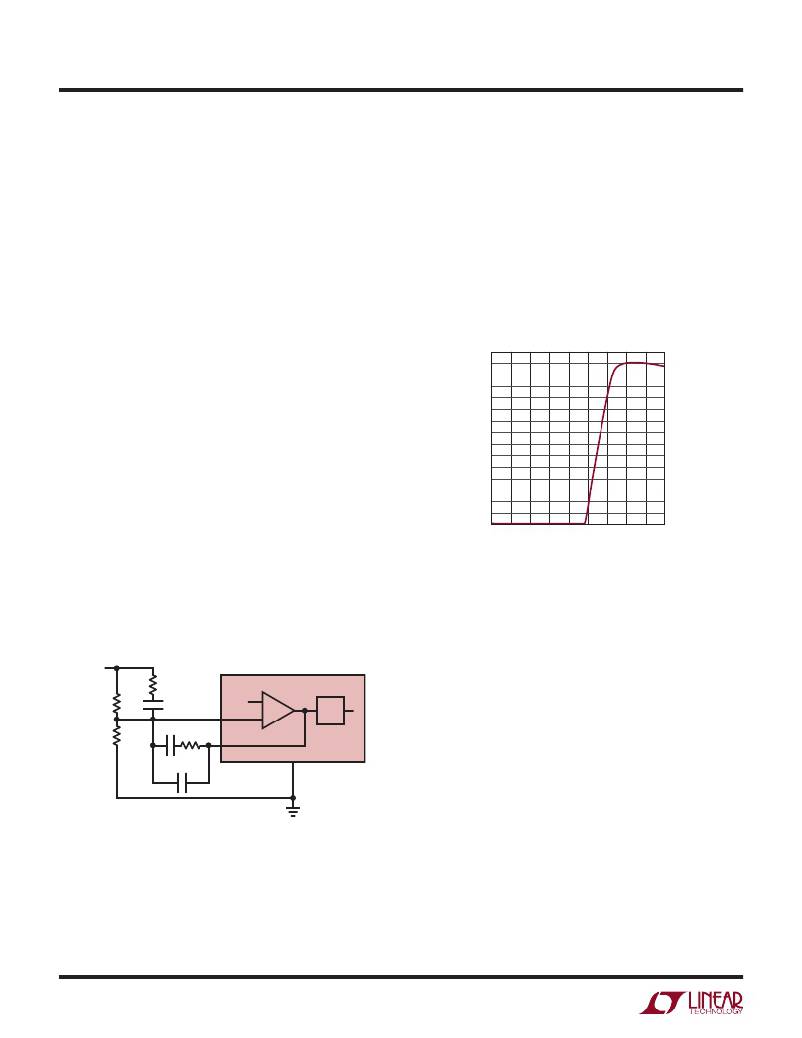
�0� 0.5� 1� 1.5� 2� 2.5� 3� 3.5� 4� 4.5�
�CURRENT� OUT� OF� SW1� PIN� (A)�
�3536� F03�
�Figure� 3.� FB� Current� for� Input� Current� Limitation�
�Since� this� input� current� limit� circuit� maintains� the� error�
�amplifier� in� an� active� state� it� ensures� a� smooth� recovery�
�and� minimal� overshoot� once� the� current� limit� fault� condi-�
�tion� is� removed.� On� a� hard� output� short,� it� is� possible� for�
�the� inductor� current� to� increase� substantially� beyond� the�
�current� limit� threshold� before� the� input� current� limit� has�
�time� to� react� and� reduce� the� inductor� current.� For� this�
�reason,� there� is� a� second� current� limit� circuit� (peak� cur-�
�rent� limit),� which� turns� off� power� switch� A� if� the� current�
�through� switch� A� exceeds� the� approximately� 3.4A� limit�
�threshold.� This� provides� additional� protection� in� the� case� of�
�an� instantaneous� hard� output� short� and� provides� time� for�
�the� primary� current� limit� to� react.� When� the� input� voltage�
�is� lower� than� 2.4V,� the� input� and� peak� current� limit� thresh-�
�olds� are� gradually� decreased.� For� minimum� input� voltage�
�(1.8V)� they� are� typically� 1.7A� and� 2.3A� respectively.� See�
�the� Typical� Performance� Characteristics� and� the� Inductor�
�Selection� section� for� information� about� the� inductor� value�
�for� maximum� output� current� capability.�
�3536fa�
�10�
�相关PDF资料 |
PDF描述 |
|---|---|
| LTC3521EUF#PBF | IC REG BUCK BOOST SYNC ADJ 24QFN |
| LT3695EMSE-3.3#PBF | IC REG BUCK 3.3V 1A 16MSOP |
| V110B15C150B2 | CONVERTER MOD DC/DC 15V 150W |
| V110B12E200BG2 | CONVERTER MOD DC/DC 12V 200W |
| V110B12E200BG | CONVERTER MOD DC/DC 12V 200W |
相关代理商/技术参数 |
参数描述 |
|---|---|
| LTC3537 | 制造商:LINER 制造商全称:Linear Technology 功能描述:2.2 MHz, 600mA Synchronous Step-Up DC/DC Converter and 100mA LDO |
| LTC3537EUD#PBF | 功能描述:IC REG DL BST/LINEAR SYNC 16-QFN RoHS:是 类别:集成电路 (IC) >> PMIC - 稳压器 - 线性 + 切换式 系列:- 标准包装:2,500 系列:- 拓扑:降压(降压)同步(3),线性(LDO)(2) 功能:任何功能 输出数:5 频率 - 开关:300kHz 电压/电流 - 输出 1:控制器 电压/电流 - 输出 2:控制器 电压/电流 - 输出 3:控制器 带 LED 驱动器:无 带监控器:无 带序列发生器:是 电源电压:5.6 V ~ 24 V 工作温度:-40°C ~ 85°C 安装类型:* 封装/外壳:* 供应商设备封装:* 包装:* |
| LTC3537EUD#TRPBF | 功能描述:IC REG DL BST/LINEAR SYNC 16-QFN RoHS:是 类别:集成电路 (IC) >> PMIC - 稳压器 - 线性 + 切换式 系列:- 标准包装:2,500 系列:- 拓扑:降压(降压)同步(3),线性(LDO)(2) 功能:任何功能 输出数:5 频率 - 开关:300kHz 电压/电流 - 输出 1:控制器 电压/电流 - 输出 2:控制器 电压/电流 - 输出 3:控制器 带 LED 驱动器:无 带监控器:无 带序列发生器:是 电源电压:5.6 V ~ 24 V 工作温度:-40°C ~ 85°C 安装类型:* 封装/外壳:* 供应商设备封装:* 包装:* |
| LTC3537EUD-PBF | 制造商:LINER 制造商全称:Linear Technology 功能描述:2.2 MHz, 600mA Synchronous Step-Up DC/DC Converter and 100mA LDO |
| LTC3537EUD-TRPBF | 制造商:LINER 制造商全称:Linear Technology 功能描述:2.2 MHz, 600mA Synchronous Step-Up DC/DC Converter and 100mA LDO |
发布紧急采购,3分钟左右您将得到回复。