- 您现在的位置:买卖IC网 > PDF目录1830 > LTC3539EDCB-2#TRPBF (Linear Technology)IC REG BOOST SYNC ADJ 2A 8DFN PDF资料下载
参数资料
| 型号: | LTC3539EDCB-2#TRPBF |
| 厂商: | Linear Technology |
| 文件页数: | 6/14页 |
| 文件大小: | 0K |
| 描述: | IC REG BOOST SYNC ADJ 2A 8DFN |
| 标准包装: | 2,500 |
| 类型: | 升压(升压) |
| 输出类型: | 可调式 |
| 输出数: | 1 |
| 输出电压: | 1.5 V ~ 5.25 V |
| 输入电压: | 0.5 V ~ 5 V |
| PWM 型: | 电流模式,混合 |
| 频率 - 开关: | 2MHz |
| 电流 - 输出: | 2A |
| 同步整流器: | 是 |
| 工作温度: | -40°C ~ 85°C |
| 安装类型: | 表面贴装 |
| 封装/外壳: | 8-WFDFN 裸露焊盘 |
| 包装: | 带卷 (TR) |
| 供应商设备封装: | 8-DFN(3x2) |
�� �
�
�LTC3539/LTC3539-2�
�PIN� FUNCTIONS�
�SW� (Pin� 1):� Switch� Pin.� Connect� inductor� between� SW�
�and� V� IN� .� Keep� PCB� trace� lengths� as� short� and� wide� as� pos-�
�sible� to� reduce� EMI.� If� the� inductor� current� falls� to� zero,�
�or� SHDN� is� low,� an� internal� anti-ring� resistor� is� connected�
�from� SW� to� V� IN� to� minimize� EMI.�
�PGND� (Pin� 2),� GND� (Pin� 3):� Signal� and� Power� Ground.�
�Provide� a� short� direct� PCB� path� between� PGND,� GND� and�
�the� (–)� side� of� the� input� and� output� capacitors.�
�V� IN� (Pin� 4):� Battery� Input� Voltage.� Connect� a� minimum� of�
�2.2μF� ceramic� decoupling� capacitor� from� this� pin� to� ground.�
�SHDN� (Pin� 5):� Logic� Controlled� Shutdown� Input.� There�
�is� an� internal� 4M� pull-down� on� this� pin.�
�SHDN� =� High:� Normal� operation.�
�SHDN� =� Low:� Shutdown,� quiescent� current� <1μA.�
�FB� (Pin� 6):� Feedback� Input� to� the� g� m� Error� Amplifier.�
�Connect� resistor� divider� tap� to� this� pin.� The� output� volt-�
�age� can� be� adjusted� from� 1.5V� to� 5.25V� by:� V� OUT� =� 1.20V�
�?� [1� +� (� R2/R1)]�
�MODE� (Pin� 7):� Burst� Mode� Pin.� A� logic� controlled� input�
�to� select� either� automatic� Burst� Mode� operation� or� forced�
�fixed� frequency� operation.�
�MODE� =� High:� Burst� Mode� operation� at� light� loads�
�MODE� =� Low:� Fixed� frequency� PWM� Mode�
�V� OUT� (Pin� 8):� Output� Voltage� Sense� and� Drain� of� the�
�Internal� Synchronous� Rectifier.� PCB� trace� length� from�
�V� OUT� to� the� output� filter� capacitor� should� be� as� short� and�
�wide� as� possible.�
�Exposed� Pad� (Pin� 9):� The� exposed� pad� must� be� soldered�
�to� the� PCB� ground� plane.� It� serves� as� another� ground�
�connection,� and� as� a� means� of� conducting� heat� away�
�from� the� die.�
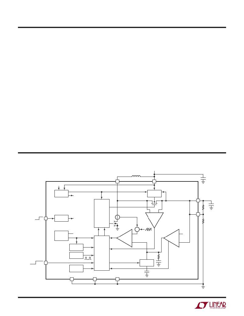
�BLOCK� DIAGRAM�
�V� IN�
�V� OUT�
�1�
�SW�
�4�
�V� IN�
�V� BEST�
�V� B�
�V� SEL�
�WELL�
�SWITCH�
�8�
�V� OUT�
�V� OUT�
�OFF� ON�
�5�
�SHDN�
�SHUTDOWN�
�SHUTDOWN�
�GATE� DRIVERS�
�AND�
�ANTI-CROSS�
�CONDUCTION�
�I� PK�
�COMPARATOR�
�Σ�
�I� ZERO�
�COMPARATOR�
�FB�
�6�
�R2�
�R1�
�V� REF�
�UVLO�
�V� REF�
�UVLO�
�I� PK�
�SLOPE�
�COMPARATOR�
�V� REF�
�FB�
�PWM� BURST�
�7�
�START-UP�
�1MHz/2MHz�
�OSC�
�CLK�
�LOGIC� AND�
�BURST� MODE�
�CONTROL�
�I� ZERO�
�BURST�
�CLAMP�
�ERROR�
�AMPLIFIER/SLEEP�
�COMPARATOR�
�MODE�
�THERMAL�
�SHUTDOWN�
�TSD�
�WAKE�
�SOFT-START�
�9�
�EXPOSED� PAD�
�2�
�PGND�
�3�
�GND�
�3539� BD�
�35392fb�
�6�
�For� more� information� www.linear.com/3539/3539-2�
�相关PDF资料 |
PDF描述 |
|---|---|
| LTC3542IDC#TRMPBF | IC REG BUCK SYNC ADJ 0.5A 6DFN |
| LTC3543EDCB#TRPBF | IC REG BUCK SYNC ADJ 0.6A 8DFN |
| LTC3544BEUD#TRPBF | IC REG BUCK SYNC ADJ QUAD 16QFN |
| LTC3545IUD-1#TRPBF | IC REG BUCK SYNC ADJ 0.8A 16QFN |
| LTC3546IFE#TRPBF | IC REG BUCK SYNC ADJ DL 28TSSOP |
相关代理商/技术参数 |
参数描述 |
|---|---|
| LTC3539EDCB-PBF | 制造商:LINER 制造商全称:Linear Technology 功能描述:2A, 1MHz/2MHz Synchronous Step-Up DC/DC Converters |
| LTC3539EDCBTRMPBF | 制造商:Linear Technology 功能描述:DC-DC Converter Step-Up 0.5-5V DFN8EP |
| LTC3539EDCB-TRPBF | 制造商:LINER 制造商全称:Linear Technology 功能描述:2A, 1MHz/2MHz Synchronous Step-Up DC/DC Converters |
| LTC3541 | 制造商:LINER 制造商全称:Linear Technology 功能描述:High Efficiency Buck + VLDO Regulator |
| LTC3541-1 | 制造商:LINER 制造商全称:Linear Technology 功能描述:High Efficiency Buck + VLDO Regulator |
发布紧急采购,3分钟左右您将得到回复。