- 您现在的位置:买卖IC网 > PDF目录14133 > LTC3543EDCB#TRMPBF (Linear Technology)IC REG BUCK SYNC ADJ 0.6A 8DFN PDF资料下载
参数资料
| 型号: | LTC3543EDCB#TRMPBF |
| 厂商: | Linear Technology |
| 文件页数: | 15/20页 |
| 文件大小: | 0K |
| 描述: | IC REG BUCK SYNC ADJ 0.6A 8DFN |
| 标准包装: | 500 |
| 类型: | 降压(降压) |
| 输出类型: | 可调式 |
| 输出数: | 1 |
| 输出电压: | 0.6 V ~ 5.5 V |
| 输入电压: | 2.5 V ~ 5.5 V |
| PWM 型: | 电流模式,混合 |
| 频率 - 开关: | 2.25MHz |
| 电流 - 输出: | 600mA |
| 同步整流器: | 是 |
| 工作温度: | -40°C ~ 85°C |
| 安装类型: | 表面贴装 |
| 封装/外壳: | 8-WFDFN 裸露焊盘 |
| 包装: | 带卷 (TR) |
| 供应商设备封装: | 8-DFN(3x2) |
�� �
�
�LTC3543�
�APPLICATIONS� INFORMATION�
�Checking� Transient� Response�
�The� regulator� loop� response� can� be� checked� by� looking�
�at� the� load� transient� response.� Switching� regulators� take�
�several� cycles� to� respond� to� a� step� in� load� current.� When�
�a� load� step� occurs,� V� OUT� immediately� shifts� by� an� amount�
�equal� to� (� Δ� I� LOAD� ?� ESR),� where� ESR� is� the� effective� series�
�resistance� of� C� OUT� .� Δ� I� LOAD� also� begins� to� charge� or� dis-�
�charge� C� OUT� ,� which� generates� a� feedback� error� signal.�
�The� regulator� loop� then� acts� to� return� V� OUT� to� its� steady�
�state� value.� During� this� recovery� time,� V� OUT� can� be� moni-�
�tored� for� overshoot� or� ringing� that� would� indicate� a� stability�
�problem.� For� a� detailed� explanation� of� the� switching� control�
�loop� theory,� see� Application� Note� 76.�
�A� second,� more� severe� transient� is� caused� by� switching�
�in� loads� with� large� (>1μF)� supply� bypass� capacitors.� The�
�discharged� bypass� capacitors� are� effectively� put� in� paral-�
�lel� with� C� OUT� ,� causing� a� rapid� drop� in� V� OUT� .� No� regulator�
�can� deliver� enough� current� to� prevent� this� problem� if� the�
�load� switch� resistance� is� low� and� it� is� driven� quickly.� The�
�only� solution� is� to� limit� the� rise� time� of� the� switch� drive�
�so� that� the� load� rise� time� is� limited� to� approximately�
�25� ?� C� LOAD� .� Thus,� a� 10μF� capacitor� charging� to� 3.3V� would�
�require� a� 250μs� rise� time,� limiting� the� charging� current�
�to� about� 130mA.�
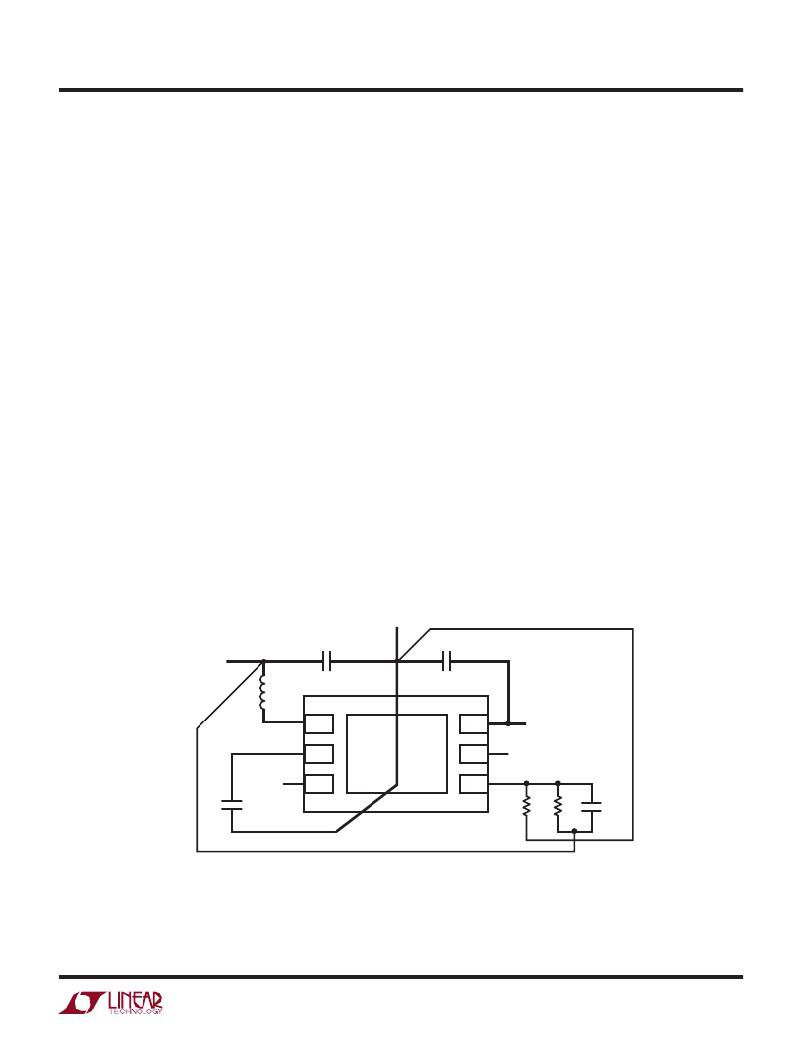
�GND�
�PC� Board� Layout� Checklist�
�When� laying� out� the� printed� circuit� board,� the� follow-�
�ing� checklist� should� be� used� to� ensure� proper� opera-�
�tion� of� the� LTC3543.� These� items� are� also� illustrated�
�graphically� in� Figures� 5� and� 6.� Check� the� following� in�
�your� layout:�
�1.� The� power� traces,� consisting� of� the� GND� trace,� the� SW�
�trace,� and� the� V� IN� trace� should� be� kept� short,� direct�
�and� wide.�
�2.� Does� the� V� FB� pin� connect� directly� to� the� feedback� volt-�
�age� reference?� Ensure� that� there� is� no� load� current�
�running� from� the� feedback� reference� voltage� and� the�
�V� FB� pin.�
�3.� Does� the� (+)� plate� of� C� IN� connect� to� V� IN� as� closely� as�
�possible?� This� capacitor� provides� the� AC� current� to� the�
�internal� power� MOSFETs.�
�4.� Keep� the� switching� node,� SW,� away� from� the� sensitive�
�V� FB� node.�
�5.� Keep� the� (–)� plates� of� C� IN� and� C� OUT� as� close� as� pos-�
�sible.�
�V� OUT�
�C� OUT�
�+� –�
�–�
�C� IN�
�+�
�L�
�SW�
�CAP�
�V� IN�
�RUN�
�V� IN�
�C1�
�MODE�
�V� FB�
�R1�
�R2�
�–�
�C� FWD�
�+�
�3543� F05�
�Figure� 5.� LTC3543� Layout� Diagram�
�3543fa�
�15�
�相关PDF资料 |
PDF描述 |
|---|---|
| HM66A-0630120NLF13 | SHIELDED POWER INDUCTORS |
| VI-J42-CZ-F1 | CONVERTER MOD DC/DC 15V 25W |
| HM66A-0630100NLF13 | SHIELDED POWER INDUCTORS |
| LTC3531EDD-3#PBF | IC REG BUCK BST SYNC 3V .2A 8DFN |
| HM66A-06308R0NLF13 | SHIELDED POWER INDUCTORS |
相关代理商/技术参数 |
参数描述 |
|---|---|
| LTC3544 | 制造商:LINER 制造商全称:Linear Technology 功能描述:Quad Synchronous Step-Down Regulator: 2.25MHz, 300mA, 200mA, 200mA, 100mA |
| LTC3544B | 制造商:LINER 制造商全称:Linear Technology 功能描述:Quad Synchronous Step-Down Regulator: 2.25MHz, 300mA, 200mA, 200mA, 100mA |
| LTC3544BEUD | 制造商:LINER 制造商全称:Linear Technology 功能描述:Quad Synchronous Step-Down Regulator: 2.25MHz, 300mA, 200mA, 200mA, 100mA |
| LTC3544BEUD#PBF | 功能描述:IC REG BUCK SYNC ADJ QUAD 16QFN RoHS:是 类别:集成电路 (IC) >> PMIC - 稳压器 - DC DC 开关稳压器 系列:- 标准包装:250 系列:- 类型:降压(降压) 输出类型:固定 输出数:1 输出电压:1.2V 输入电压:2.05 V ~ 6 V PWM 型:电压模式 频率 - 开关:2MHz 电流 - 输出:500mA 同步整流器:是 工作温度:-40°C ~ 85°C 安装类型:表面贴装 封装/外壳:6-UFDFN 包装:带卷 (TR) 供应商设备封装:6-SON(1.45x1) 产品目录页面:1032 (CN2011-ZH PDF) 其它名称:296-25628-2 |
| LTC3544BEUD#TRPBF | 功能描述:IC REG BUCK SYNC ADJ QUAD 16QFN RoHS:是 类别:集成电路 (IC) >> PMIC - 稳压器 - DC DC 开关稳压器 系列:- 标准包装:2,500 系列:- 类型:降压(降压) 输出类型:固定 输出数:1 输出电压:1.2V,1.5V,1.8V,2.5V 输入电压:2.7 V ~ 20 V PWM 型:- 频率 - 开关:- 电流 - 输出:50mA 同步整流器:是 工作温度:-40°C ~ 125°C 安装类型:表面贴装 封装/外壳:10-TFSOP,10-MSOP(0.118",3.00mm 宽)裸露焊盘 包装:带卷 (TR) 供应商设备封装:10-MSOP 裸露焊盘 |
发布紧急采购,3分钟左右您将得到回复。