- 您现在的位置:买卖IC网 > PDF目录1830 > LTC3548IMSE#TRPBF (Linear Technology)IC REG BUCK SYNC ADJ DL 10MSOP PDF资料下载
参数资料
| 型号: | LTC3548IMSE#TRPBF |
| 厂商: | Linear Technology |
| 文件页数: | 6/16页 |
| 文件大小: | 0K |
| 描述: | IC REG BUCK SYNC ADJ DL 10MSOP |
| 标准包装: | 2,500 |
| 类型: | 降压(降压) |
| 输出类型: | 可调式 |
| 输出数: | 2 |
| 输出电压: | 0.6 V ~ 5 V |
| 输入电压: | 2.5 V ~ 5.5 V |
| PWM 型: | 电流模式,混合 |
| 频率 - 开关: | 2.25MHz |
| 电流 - 输出: | 400mA,800mA |
| 同步整流器: | 是 |
| 工作温度: | -40°C ~ 85°C |
| 安装类型: | 表面贴装 |
| 封装/外壳: | 10-TFSOP,10-MSOP(0.118",3.00mm 宽)裸露焊盘 |
| 包装: | 带卷 (TR) |
| 供应商设备封装: | 10-MSOP 裸露焊盘 |
�� �
�
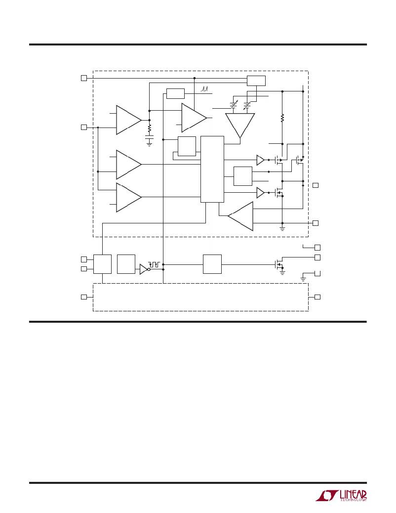
�LTC3548�
�BLOCK� DIAGRAM�
�REGULATOR� 1�
�MODE/SYNC�
�6�
�BURST�
�CLAMP�
�V� IN�
�SLOPE�
�COMP�
�V� FB1�
�1�
�0.6V�
�+�
�–�
�EA�
�I� TH�
�0.35V�
�–�
�+�
�EN�
�BURST�
�SLEEP�
�–�
�I� COMP�
�+�
�5Ω�
�S�
�R�
�RS�
�LATCH�
�Q�
�Q�
�0.55V�
�–�
�+�
�UVDET�
�UV�
�SWITCHING�
�LOGIC�
�AND�
�BLANKING�
�CIRCUIT�
�ANTI�
�SHOOT-�
�THRU�
�4� SW1�
�+�
�OVDET�
�OV�
�0.65V�
�–�
�SHUTDOWN�
�PGOOD1�
�I� RCMP�
�V� IN�
�11� GND�
�3� V� IN�
�RUN1�
�RUN2�
�2�
�9�
�0.6V� REF�
�OSC�
�OSC�
�POR�
�COUNTER�
�8� POR�
�5� GND�
�PGOOD2�
�REGULATOR� 2� (IDENTICAL� TO� REGULATOR� 1)�
�V� FB2�
�10�
�7� SW2�
�3548� BD�
�OPERATION�
�The� LTC3548� uses� a� constant-frequency,� current� mode�
�architecture.� The� operating� frequency� is� set� at� 2.25MHz�
�and� can� be� synchronized� to� an� external� oscillator.� Both�
�channels� share� the� same� clock� and� run� in-phase.� To� suit� a�
�variety� of� applications,� the� selectable� Mode� pin� allows� the�
�user� to� choose� between� low� noise� and� high� ef?ciency.�
�The� output� voltage� is� set� by� an� external� divider� returned�
�to� the� V� FB� pins.� An� error� ampli?er� compares� the� divided�
�output� voltage� with� a� reference� voltage� of� 0.6V� and� adjusts�
�the� peak� inductor� current� accordingly.� An� undervoltage�
�comparator� will� pull� the� POR� output� low� if� the� output�
�voltage� is� not� above� –8.5%� of� the� reference� voltage.� The�
�POR� output� will� go� high� after� 262,144� clock� cycles� (about�
�117ms)� of� achieving� regulation.�
�Main� Control� Loop�
�During� normal� operation,� the� top� power� switch� (P-channel�
�MOSFET)� is� turned� on� at� the� beginning� of� a� clock� cycle�
�when� the� V� FB� voltage� is� below� the� the� reference� voltage.�
�The� current� into� the� inductor� and� the� load� increases� until�
�the� current� limit� is� reached.� The� switch� turns� off� and�
�energy� stored� in� the� inductor� ?ows� through� the� bottom�
�switch� (N-channel� MOSFET)� into� the� load� until� the� next�
�clock� cycle.�
�The� peak� inductor� current� is� controlled� by� the� internally�
�compensated� I� TH� voltage,� which� is� the� output� of� the�
�error� ampli?er.This� ampli?er� compares� the� V� FB� pin� to�
�the� 0.6V� reference.� When� the� load� current� increases,�
�the� V� FB� voltage� decreases� slightly� below� the� reference.�
�3548fc�
�6�
�相关PDF资料 |
PDF描述 |
|---|---|
| LTC3549EDCB#TRPBF | IC REG BUCK SYNC ADJ 0.25A 6DFN |
| LTC3550EDHC-1#TRPBF | IC CHARGER BATT DUAL 16-DFN |
| LTC3552EDHC-1#TRPBF | IC CHARGER BATT LI-ION 16-DFN |
| LTC3559EUD-1#TRPBF | IC USB BATTERY CHARGER 16-QFN |
| LTC3560IS6#TRPBF | IC REG BUCK SYNC ADJ TSOT23-6 |
相关代理商/技术参数 |
参数描述 |
|---|---|
| LTC3549 | 制造商:LINER 制造商全称:Linear Technology 功能描述:250mA Low VIN Buck Regulator in 2mm × 3mm DFN |
| LTC3549EDCB | 制造商:LINER 制造商全称:Linear Technology 功能描述:250mA Low VIN Buck Regulator in 2mm × 3mm DFN |
| LTC3549EDCB#PBF | 制造商:Linear Technology 功能描述:VOLTAGE REGULATOR BUCK 2.25M 制造商:Linear Technology 功能描述:VOLTAGE REGULATOR, BUCK, 2.25MHZ, 250mA, DFN-6; Primary Input Voltage:5.5V; No. of Outputs:1; Output Current:250mA; No. of Pins:6; Operating Temperature Min:-40C; Operating Temperature Max:85C; Package / Case:6-DFN ;RoHS Compliant: Yes |
| LTC3549EDCB#TRM | 制造商:Linear Technology 功能描述:250MA, LOW VIN BUCK REGULATOR |
| LTC3549EDCB#TRMPBF | 功能描述:IC REG BUCK SYNC ADJ 0.25A 6DFN RoHS:是 类别:集成电路 (IC) >> PMIC - 稳压器 - DC DC 开关稳压器 系列:- 产品培训模块:High Efficiency Current Mode Switching Regulators CMOS LDO Regulators 特色产品:BD91x Series Step-Down Regulators 标准包装:2,500 系列:- 类型:降压(降压) 输出类型:两者兼有 输出数:2 输出电压:3.3V,0.8 V ~ 2.5 V 输入电压:4.5 V ~ 5.5 V PWM 型:电流模式 频率 - 开关:1MHz 电流 - 输出:1.5A 同步整流器:是 工作温度:-40°C ~ 85°C 安装类型:表面贴装 封装/外壳:20-VFQFN 裸露焊盘 包装:带卷 (TR) 供应商设备封装:VQFN020V4040 产品目录页面:1373 (CN2011-ZH PDF) 其它名称:BD9152MUV-E2TR |
发布紧急采购,3分钟左右您将得到回复。