- 您现在的位置:买卖IC网 > PDF目录1830 > LTC3548IMSE#TRPBF (Linear Technology)IC REG BUCK SYNC ADJ DL 10MSOP PDF资料下载
参数资料
| 型号: | LTC3548IMSE#TRPBF |
| 厂商: | Linear Technology |
| 文件页数: | 8/16页 |
| 文件大小: | 0K |
| 描述: | IC REG BUCK SYNC ADJ DL 10MSOP |
| 标准包装: | 2,500 |
| 类型: | 降压(降压) |
| 输出类型: | 可调式 |
| 输出数: | 2 |
| 输出电压: | 0.6 V ~ 5 V |
| 输入电压: | 2.5 V ~ 5.5 V |
| PWM 型: | 电流模式,混合 |
| 频率 - 开关: | 2.25MHz |
| 电流 - 输出: | 400mA,800mA |
| 同步整流器: | 是 |
| 工作温度: | -40°C ~ 85°C |
| 安装类型: | 表面贴装 |
| 封装/外壳: | 10-TFSOP,10-MSOP(0.118",3.00mm 宽)裸露焊盘 |
| 包装: | 带卷 (TR) |
| 供应商设备封装: | 10-MSOP 裸露焊盘 |
�� �
�
�LTC3548�
�APPLICATIONS� INFORMATION�
�The� inductor� value� will� also� have� an� effect� on� Burst� Mode�
�operation.� The� transition� from� low� current� operation�
�begins� when� the� peak� inductor� current� falls� below� a� level�
�set� by� the� burst� clamp.� Lower� inductor� values� result� in�
�higher� ripple� current� which� causes� this� to� occur� at� lower�
�load� currents.� This� causes� a� dip� in� ef?ciency� in� the� upper�
�range� of� low� current� operation.� In� Burst� Mode� operation,�
�lower� inductance� values� will� cause� the� burst� frequency�
�required.� Several� capacitors� may� also� be� paralleled� to� meet�
�the� size� or� height� requirements� of� the� design.� An� additional�
�0.1μF� to� 1μF� ceramic� capacitor� is� also� recommended� on�
�V� IN� for� high� frequency� decoupling,� when� not� using� an� all�
�ceramic� capacitor� solution.�
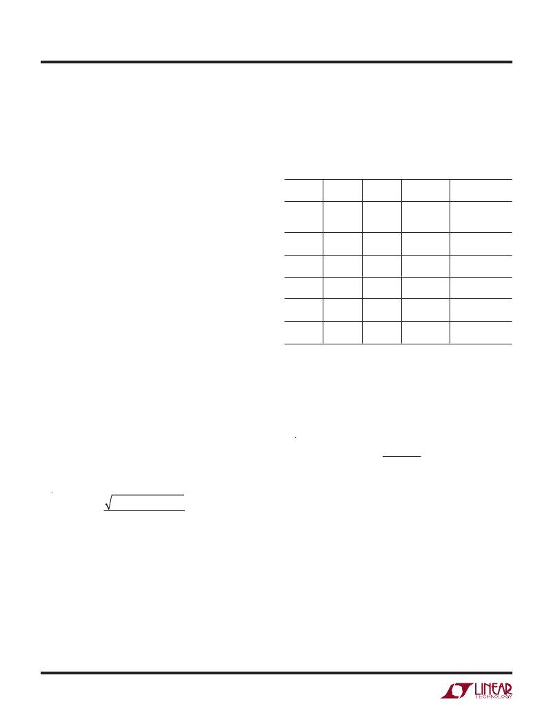
�Table� 1.� Representation� Surface� Mount� Inductors�
�PART� VALUE� DCR� MAX� DC� SIZE�
�NUMBER� (μH)� (Ω� MAX)� CURRENT� (A)� W� ×� L� ×� H� (mm� 3� )�
�to� increase.�
�Sumida�
�2.2�
�0.075�
�1.20�
�3.8� � 3.8� � 1.8�
�Inductor� Core� Selection�
�CDRH3D16�
�3.3�
�4.7�
�0.110�
�0.162�
�1.10�
�0.90�
�Different� core� materials� and� shapes� will� change� the� size/�
�current� and� price/current� relationship� of� an� inductor.� Toroid�
�or� shielded� pot� cores� in� ferrite� or� permalloy� materials� are�
�small� and� do� not� radiate� much� energy,� but� generally� cost�
�more� than� powdered� iron� core� inductors� with� similar� elec-�
�trical� characteristics.� The� choice� of� which� style� inductor� to�
�use� often� depends� more� on� the� price� vs� size� requirements�
�and� any� radiated� ?eld/EMI� requirements� than� on� what� the�
�Sumida�
�CDRH2D11�
�Sumida�
�CMD4D11�
�Murata�
�LQH32CN�
�Toko�
�D312F�
�Panasonic�
�ELT5KT�
�1.5�
�2.2�
�2.2�
�3.3�
�1.0�
�2.2�
�2.2�
�3.3�
�3.3�
�4.7�
�0.068�
�0.170�
�0.116�
�0.174�
�0.060�
�0.097�
�0.060�
�0.260�
�0.17�
�0.20�
�0.900�
�0.780�
�0.950�
�0.770�
�1.00�
�0.079�
�1.08�
�0.92�
�1.00�
�0.95�
�3.2� � 3.2� � 1.2�
�4.4� � 5.8� � 1.2�
�2.5� � 3.2� � 2.0�
�2.5� � 3.2� � 2.0�
�4.5� � 5.4� � 1.2�
�LTC3548� requires� to� operate.� Table� 1� shows� some� typi-�
�cal� surface� mount� inductors� that� work� well� in� LTC3548�
�applications.�
�Input� Capacitor� (C� IN� )� Selection�
�In� continuous� mode,� the� input� current� of� the� converter� is� a�
�square� wave� with� a� duty� cycle� of� approximately� V� OUT� /V� IN� .�
�Output� Capacitor� (C� OUT� )� Selection�
�The� selection� of� C� OUT� is� driven� by� the� required� ESR� to�
�minimize� voltage� ripple� and� load� step� transients.� Typically,�
�once� the� ESR� requirement� is� satis?ed,� the� capacitance�
�is� adequate� for� ?ltering.� The� output� ripple� (ΔV� OUT� )� is�
�determined� by:�
�Δ� V� OUT� ≈� Δ� I� L� ?� ESR� +�
�Topreventlargevoltagetransients,alowequivalentseries�
�resistance� (ESR)� input� capacitor� sized� for� the� maximum�
�RMS� current� must� be� used.� The� maximum� RMS� capacitor�
�?�
�?�
�1� ?�
�8f� O� C� OUT� ?� ?�
�current� is� given� by:�
�where� f� =� operating� frequency,� C� OUT� =� output� capacitance�
�I� RMS� ≈� I� MAX�
�V� OUT� (V� IN� –� V� OUT� )�
�V� IN�
�and� ΔI� L� =� ripple� current� in� the� inductor.� The� output� ripple�
�is� highest� at� maximum� input� voltage� since� ΔI� L� increases�
�with� input� voltage.� With� ΔI� L� =� 0.3� ?� I� OUT(MAX)� the� output�
�where� the� maximum� average� output� current� I� MAX� equals�
�the� peak� current� minus� half� the� peak-to-peak� ripple� cur-�
�rent,� I� MAX� =� I� LIM� –� ΔI� L� /2.�
�This� formula� has� a� maximum� at� V� IN� =� 2V� OUT� ,� where� I� RMS�
�=� I� OUT� /2.� This� simple� worst-case� is� commonly� used� to�
�design� because� even� signi?cant� deviations� do� not� offer�
�much� relief.� Note� that� capacitor� manufacturer’s� ripple� cur-�
�rent� ratings� are� often� based� on� only� 2000� hours� lifetime.�
�This� makes� it� advisable� to� further� derate� the� capacitor,�
�or� choose� a� capacitor� rated� at� a� higher� temperature� than�
�8�
�ripple� will� be� less� than� 100mV� at� maximum� V� IN� and�
�f� O� =� 2.25MHz� with:�
�ESR� COUT� <� 150m�
�Once� the� ESR� requirements� for� C� OUT� have� been� met,� the�
�RMS� current� rating� generally� far� exceeds� the� I� RIPPLE(P-P)�
�requirement,� except� for� an� all� ceramic� solution.�
�In� surface� mount� applications,� multiple� capacitors� may�
�have� to� be� paralleled� to� meet� the� capacitance,� ESR� or�
�RMS� current� handling� requirement� of� the� application.�
�Aluminum� electrolytic,� special� polymer,� ceramic� and� dry�
�3548fc�
�相关PDF资料 |
PDF描述 |
|---|---|
| LTC3549EDCB#TRPBF | IC REG BUCK SYNC ADJ 0.25A 6DFN |
| LTC3550EDHC-1#TRPBF | IC CHARGER BATT DUAL 16-DFN |
| LTC3552EDHC-1#TRPBF | IC CHARGER BATT LI-ION 16-DFN |
| LTC3559EUD-1#TRPBF | IC USB BATTERY CHARGER 16-QFN |
| LTC3560IS6#TRPBF | IC REG BUCK SYNC ADJ TSOT23-6 |
相关代理商/技术参数 |
参数描述 |
|---|---|
| LTC3549 | 制造商:LINER 制造商全称:Linear Technology 功能描述:250mA Low VIN Buck Regulator in 2mm × 3mm DFN |
| LTC3549EDCB | 制造商:LINER 制造商全称:Linear Technology 功能描述:250mA Low VIN Buck Regulator in 2mm × 3mm DFN |
| LTC3549EDCB#PBF | 制造商:Linear Technology 功能描述:VOLTAGE REGULATOR BUCK 2.25M 制造商:Linear Technology 功能描述:VOLTAGE REGULATOR, BUCK, 2.25MHZ, 250mA, DFN-6; Primary Input Voltage:5.5V; No. of Outputs:1; Output Current:250mA; No. of Pins:6; Operating Temperature Min:-40C; Operating Temperature Max:85C; Package / Case:6-DFN ;RoHS Compliant: Yes |
| LTC3549EDCB#TRM | 制造商:Linear Technology 功能描述:250MA, LOW VIN BUCK REGULATOR |
| LTC3549EDCB#TRMPBF | 功能描述:IC REG BUCK SYNC ADJ 0.25A 6DFN RoHS:是 类别:集成电路 (IC) >> PMIC - 稳压器 - DC DC 开关稳压器 系列:- 产品培训模块:High Efficiency Current Mode Switching Regulators CMOS LDO Regulators 特色产品:BD91x Series Step-Down Regulators 标准包装:2,500 系列:- 类型:降压(降压) 输出类型:两者兼有 输出数:2 输出电压:3.3V,0.8 V ~ 2.5 V 输入电压:4.5 V ~ 5.5 V PWM 型:电流模式 频率 - 开关:1MHz 电流 - 输出:1.5A 同步整流器:是 工作温度:-40°C ~ 85°C 安装类型:表面贴装 封装/外壳:20-VFQFN 裸露焊盘 包装:带卷 (TR) 供应商设备封装:VQFN020V4040 产品目录页面:1373 (CN2011-ZH PDF) 其它名称:BD9152MUV-E2TR |
发布紧急采购,3分钟左右您将得到回复。