- 您现在的位置:买卖IC网 > PDF目录1830 > LTC3560IS6#TRPBF (Linear Technology)IC REG BUCK SYNC ADJ TSOT23-6 PDF资料下载
参数资料
| 型号: | LTC3560IS6#TRPBF |
| 厂商: | Linear Technology |
| 文件页数: | 10/16页 |
| 文件大小: | 0K |
| 描述: | IC REG BUCK SYNC ADJ TSOT23-6 |
| 标准包装: | 2,500 |
| 类型: | 降压(降压) |
| 输出类型: | 可调式 |
| 输出数: | 1 |
| 输出电压: | 0.6 V ~ 5.5 V |
| 输入电压: | 2.5 V ~ 5.5 V |
| PWM 型: | 电流模式,混合 |
| 频率 - 开关: | 2.25MHz |
| 电流 - 输出: | 800mA |
| 同步整流器: | 是 |
| 工作温度: | -40°C ~ 125°C |
| 安装类型: | 表面贴装 |
| 封装/外壳: | SOT-23-6 细型,TSOT-23-6 |
| 包装: | 带卷 (TR) |
| 供应商设备封装: | TSOT-23-6 |
�� �
�
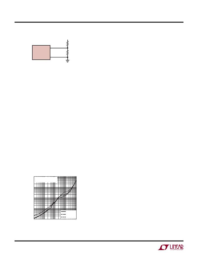
�LTC3560�
�APPLICATIONS� INFORMATION�
�0.6V� ≤� V� OUT� ≤� 5.5V�
�1.� The� V� IN� quiescent� current� is� due� to� two� components:�
�LTC3560�
�V� FB�
�GND�
�R2�
�R1�
�3560� F02�
�the� DC� bias� current� as� given� in� the� electrical� charac-�
�teristics� and� the� internal� main� switch� and� synchronous�
�switch� gate� charge� currents.� The� gate� charge� current�
�results� from� switching� the� gate� capacitance� of� the�
�internal� power� MOSFET� switches.� Each� time� the� gate�
�is� switched� from� high� to� low� to� high� again,� a� packet� of�
�Figure� 2.� Setting� the� LTC3560� Output� Voltage�
�Ef?ciency� Considerations�
�The� ef?ciency� of� a� switching� regulator� is� equal� to� the� output�
�power� divided� by� the� input� power� times� 100%.� It� is� often�
�useful� to� analyze� individual� losses� to� determine� what� is�
�limiting� the� ef?ciency� and� which� change� would� produce�
�the� most� improvement.� Ef?ciency� can� be� expressed� as:�
�Ef?ciency� =� 100%� –� (L1� +� L2� +� L3� +� ...)�
�where� L1,� L2,� etc.� are� the� individual� losses� as� a� percentage�
�of� input� power.�
�Although� all� dissipative� elements� in� the� circuit� produce�
�losses,� two� main� sources� usually� account� for� most� of�
�the� losses� in� LTC3560� circuits:� V� IN� quiescent� current� and�
�I� 2� R� losses.� The� V� IN� quiescent� current� loss� dominates�
�the� ef?ciency� loss� at� very� low� load� currents� whereas� the�
�I� 2� R� loss� dominates� the� ef?ciency� loss� at� medium� to� high�
�load� currents.� In� a� typical� ef?ciency� plot,� the� ef?ciency�
�curve� at� very� low� load� currents� can� be� misleading� since�
�the� actual� power� lost� is� of� no� consequence� as� illustrated�
�in� Figure� 3.�
�charge,� dQ,� moves� from� V� IN� to� ground.� The� resulting�
�dQ/dt� is� the� current� out� of� V� IN� that� is� typically� larger�
�than� the� DC� bias� current.� In� continuous� mode,� I� GATECHG�
�=� f(Q� T� +� Q� B� )� where� Q� T� and� Q� B� are� the� gate� charges� of�
�the� internal� top� and� bottom� switches.� Both� the� DC� bias�
�and� gate� charge� losses� are� proportional� to� V� IN� and� thus�
�their� effects� will� be� more� pronounced� at� higher� supply�
�voltages.�
�2.� I� 2� R� losses� are� calculated� from� the� resistances� of� the�
�internal� switches,� R� SW� ,� and� external� inductor� R� L� .� In�
�continuous� mode,� the� average� output� current� ?owing�
�through� inductor� L� is� “chopped”� between� the� main�
�switch� and� the� synchronous� switch.� Thus,� the� series�
�resistance� looking� into� the� SW� pin� is� a� function� of� both�
�top� and� bottom� MOSFET� R� DS(ON)� and� the� duty� cycle�
�(DC)� as� follows:�
�R� SW� =� (R� DS(ON)TOP� )(DC)� +� (R� DS(ON)BOT� )(1� –� DC)�
�The� R� DS(ON)� for� both� the� top� and� bottom� MOSFETs� can�
�be� obtained� from� the� Typical� Performance� Charateristics�
�curves.� Thus,� to� obtain� I� 2� R� losses,� simply� add� R� SW� to�
�R� L� and� multiply� the� result� by� the� square� of� the� average�
�output� current.�
�1�
�0.1�
�0.01�
�V� OUT� =� 2.5V�
�Burst� Mode� OPERATION�
�Other� losses� including� C� IN� and� C� OUT� ESR� dissipative� losses�
�and� inductor� core� losses� generally� account� for� less� than�
�2%� total� additional� loss.�
�Thermal� Considerations�
�In� most� applications� the� LTC3560� does� not� dissipate�
�much� heat� due� to� its� high� ef?ciency.� But,� in� applica-�
�0.001�
�V� IN� =� 3.6V�
�V� IN� =� 4.2V�
�tions� where� the� LTC3560� is� running� at� high� ambient�
�temperature� with� low� supply� voltage� and� high� duty� cycles,�
�0.0001�
�V� IN� =� 5.5V�
�such� as� in� dropout,� the� heat� dissipated� may� exceed� the�
�0.1�
�1�
�10� 100�
�LOAD� CURRENT� (mA)�
�1000�
�3560� F03�
�maximum� junction� temperature� of� the� part.� If� the� junction�
�temperature� reaches� approximately� 150°C,� both� power�
�Figure� 3.� Power� Lost� vs� Load� Current�
�3560fb�
�10�
�相关PDF资料 |
PDF描述 |
|---|---|
| LTC3561EDD#TRPBF | IC REG BUCK SYNC ADJ 1A 8DFN |
| LTC3562EUD#TRPBF | IC REG BUCK SYNC ADJ QUAD 20QFN |
| LTC3563EDC#TRPBF | IC REG BUCK SYNC 0.5A 6DFN |
| LTC3564IS5#TRPBF | IC REG BUCK SYNC ADJ TSOT23-5 |
| LTC3565IMSE#TRPBF | IC REG BUCK SYNC ADJ 10MSOP |
相关代理商/技术参数 |
参数描述 |
|---|---|
| LTC3561 | 制造商:LINER 制造商全称:Linear Technology 功能描述:1A, 4MHz, Synchronous Step-Down DC/DC Converter |
| LTC3561A | 制造商:LINER 制造商全称:Linear Technology 功能描述:1A, 4MHz, Synchronous Step-Down DC/DC Converter |
| LTC3561AEDD#PBF | 功能描述:IC REG BUCK SYNC ADJ 1A 8DFN RoHS:是 类别:集成电路 (IC) >> PMIC - 稳压器 - DC DC 开关稳压器 系列:- 标准包装:250 系列:- 类型:降压(降压) 输出类型:固定 输出数:1 输出电压:1.2V 输入电压:2.05 V ~ 6 V PWM 型:电压模式 频率 - 开关:2MHz 电流 - 输出:500mA 同步整流器:是 工作温度:-40°C ~ 85°C 安装类型:表面贴装 封装/外壳:6-UFDFN 包装:带卷 (TR) 供应商设备封装:6-SON(1.45x1) 产品目录页面:1032 (CN2011-ZH PDF) 其它名称:296-25628-2 |
| LTC3561AEDD#TRPBF | 功能描述:IC REG BUCK SYNC ADJ 1A 8DFN RoHS:是 类别:集成电路 (IC) >> PMIC - 稳压器 - DC DC 开关稳压器 系列:- 标准包装:2,500 系列:- 类型:升压(升压) 输出类型:可调式 输出数:1 输出电压:1.24 V ~ 30 V 输入电压:1.5 V ~ 12 V PWM 型:电流模式,混合 频率 - 开关:600kHz 电流 - 输出:500mA 同步整流器:无 工作温度:-40°C ~ 85°C 安装类型:表面贴装 封装/外壳:8-SOIC(0.154",3.90mm 宽) 包装:带卷 (TR) 供应商设备封装:8-SOIC |
| LTC3561AEDD-PBF | 制造商:LINER 制造商全称:Linear Technology 功能描述:1A, 4MHz, Synchronous Step-Down DC/DC Converter |
发布紧急采购,3分钟左右您将得到回复。