- 您现在的位置:买卖IC网 > PDF目录14824 > LTC3568EDD#PBF (Linear Technology)IC REG BUCK SYNC ADJ 1.8A 10DFN PDF资料下载
参数资料
| 型号: | LTC3568EDD#PBF |
| 厂商: | Linear Technology |
| 文件页数: | 6/18页 |
| 文件大小: | 0K |
| 描述: | IC REG BUCK SYNC ADJ 1.8A 10DFN |
| 标准包装: | 121 |
| 类型: | 降压(降压) |
| 输出类型: | 可调式 |
| 输出数: | 1 |
| 输出电压: | 0.8 V ~ 5 V |
| 输入电压: | 2.5 V ~ 5.5 V |
| PWM 型: | 电流模式,混合 |
| 频率 - 开关: | 最高 4MHz |
| 电流 - 输出: | 1.8A |
| 同步整流器: | 是 |
| 工作温度: | -40°C ~ 125°C |
| 安装类型: | 表面贴装 |
| 封装/外壳: | 10-WFDFN 裸露焊盘 |
| 包装: | 管件 |
| 供应商设备封装: | 10-DFN(3x3) |
| 产品目录页面: | 1335 (CN2011-ZH PDF) |
�� �
�
�LTC3568�
�PIN� FUNCTIONS�
�SHDN/R� T� � (Pin � 1):� Combination� Shutdown� and� Timing�
�Resistor� Pin.� The� oscillator� frequency� is� programmed� by�
�connecting� a� resistor� from� this� pin� to� ground.� Forcing�
�this� pin� to� SV� IN� causes� the� device� to� be� shut� down.� In�
�shutdown� all� functions� are� disabled.�
�SYNC/MODE (Pin 2):� Combination� Mode� Selection� and�
�Oscillator� Synchronization� Pin.� This� pin� controls� the� op-�
�eration� of� the� device.� When� tied� to� SV� IN� or� SGND,� Burst�
�Mode� operation� or� pulse� skipping� mode� is� selected,�
�respectively.� If� this� pin� is� held� at� half� of� SV� IN� ,� the� forced�
�continuous� mode� is� selected.� The� oscillation� frequency�
�can� be� syncronized� to� an� external� oscillator� applied� to�
�this� pin.� When� synchronized� to� an� external� clock� pulse�
�skip� mode� is� selected.�
�SGND � (Pin � 3):� The� Signal� Ground� Pin.� All� small� signal�
�components� and� compensation� components� should� be� con-�
�nected� to� this� ground� (see� Board� Layout� Considerations).�
�SW (Pin 4):� The� Switch� Node� Connection� to� the� Inductor.�
�This� pin� swings� from� PV� IN� to� PGND.�
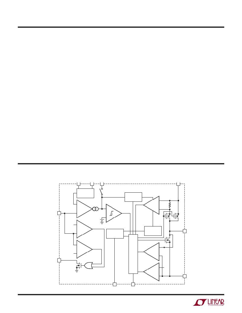
�BLOCK� DIAGRAM�
�PGND (Pin 5):� Main� Power� Ground� Pin.� Connect� to� the�
�(–)� terminal� of� C� OUT� ,� and� (–)� terminal� of� C� IN� .�
�PV� IN� (Pin 6):� Main� Supply� Pin.� Must� be� closely� decoupled�
�to� PGND.�
�SV� IN� (Pin 7):� The� Signal� Power� Pin.� All� active� circuitry�
�is� powered� from� this� pin.� Must� be� closely� decoupled� to�
�SGND.� SV� IN� must� be� greater� than� or� equal� to� PV� IN� .�
�PGOOD (Pin 8):� The� Power� Good� Pin.� This� common� drain�
�logic� output� is� pulled� to� SGND� when� the� output� voltage� is�
�not� within� ±7.5%� of� regulation.�
�V� FB� (Pin 9):� Receives� the� feedback� voltage� from� the� ex-�
�ternal� resistive� divider� across� the� output.� Nominal� voltage�
�for� this� pin� is� 0.8V.�
�I� TH� � (Pin � 10):� Error� Amplifier� Compensation� Point.� The�
�current� comparator� threshold� increases� with� this� control�
�voltage.� Nominal� voltage� range� for� this� pin� is� 0V� to� 1.5V.�
�GND � (Exposed � Pad � Pin � 11):� Thermal� Ground.� Con-�
�nect� to� SGND� and� solder� to� the� PCB� for� rated� thermal�
�performance.�
�SV� IN�
�7�
�SGND�
�3�
�I� TH�
�10�
�PV� IN�
�6�
�0.8V�
�+�
�VOLTAGE�
�REFERENCE�
�I� TH�
�LIMIT�
�BCLAMP�
�PMOS� CURRENT�
�COMPARATOR�
�+�
�V� FB� 9�
�0.74V�
�–�
�+�
�–�
�ERROR�
�AMPLIFIER�
�V� B�
�–�
�+�
�BURST�
�COMPARATOR�
�HYSTERESIS� =� 80mV�
�OSCILLATOR�
�–�
�SLOPE�
�COMPENSATION�
�4� SW�
�+�
�+�
�PGOOD� 8�
�0.86V�
�–�
�LOGIC�
�NMOS�
�COMPARATOR�
�–�
�–�
�1�
�SHDN/R� T�
�2�
�SYNC/MODE�
�REVERSE�
�COMPARATOR�
�+�
�5� PGND�
�3568� BD�
�3568fa�
� �
�相关PDF资料 |
PDF描述 |
|---|---|
| MAX6340UK21+T | IC RESET MPU LP SOT23-5 |
| 1120-470K | CHOKE RF RADIAL 47UH 10% |
| VI-JV2-EY-F1 | CONVERTER MOD DC/DC 15V 50W |
| LT1912EDD#PBF | IC REG BUCK ADJ 2A 10DFN |
| LT1172CT#PBF | IC REG MULTI CONFIG ADJ TO220 |
相关代理商/技术参数 |
参数描述 |
|---|---|
| LTC3568IDD#PBF | 功能描述:IC REG BUCK SYNC ADJ 1.8A 10DFN RoHS:是 类别:集成电路 (IC) >> PMIC - 稳压器 - DC DC 开关稳压器 系列:- 标准包装:2,500 系列:- 类型:降压(降压) 输出类型:固定 输出数:1 输出电压:1.2V,1.5V,1.8V,2.5V 输入电压:2.7 V ~ 20 V PWM 型:- 频率 - 开关:- 电流 - 输出:50mA 同步整流器:是 工作温度:-40°C ~ 125°C 安装类型:表面贴装 封装/外壳:10-TFSOP,10-MSOP(0.118",3.00mm 宽)裸露焊盘 包装:带卷 (TR) 供应商设备封装:10-MSOP 裸露焊盘 |
| LTC3568IDD#PBF | 制造商:Linear Technology 功能描述:DP-SWREG/Monolithic 4MHz 1.8A Synch St 制造商:Linear Technology 功能描述:DP-SWREG/Monolithic, 4MHz, 1.8A Synch St |
| LTC3568IDD#TRPBF | 功能描述:IC REG BUCK SYNC ADJ 1.8A 10DFN RoHS:是 类别:集成电路 (IC) >> PMIC - 稳压器 - DC DC 开关稳压器 系列:- 标准包装:2,500 系列:- 类型:降压(降压) 输出类型:固定 输出数:1 输出电压:1.2V,1.5V,1.8V,2.5V 输入电压:2.7 V ~ 20 V PWM 型:- 频率 - 开关:- 电流 - 输出:50mA 同步整流器:是 工作温度:-40°C ~ 125°C 安装类型:表面贴装 封装/外壳:10-TFSOP,10-MSOP(0.118",3.00mm 宽)裸露焊盘 包装:带卷 (TR) 供应商设备封装:10-MSOP 裸露焊盘 |
| LTC3569 | 制造商:LINER 制造商全称:Linear Technology 功能描述:7-Channel Confi gurable High Power PMIC |
| LTC3569EFE | 制造商:Linear Technology 功能描述:DC/DC Converter Chip |
发布紧急采购,3分钟左右您将得到回复。