- 您现在的位置:买卖IC网 > PDF目录13970 > LTC3569EFE#TRPBF (Linear Technology)IC REG BUCK SYNC ADJ 16TSSOP PDF资料下载
参数资料
| 型号: | LTC3569EFE#TRPBF |
| 厂商: | Linear Technology |
| 文件页数: | 14/26页 |
| 文件大小: | 0K |
| 描述: | IC REG BUCK SYNC ADJ 16TSSOP |
| 标准包装: | 2,500 |
| 类型: | 降压(降压) |
| 输出类型: | 可调式 |
| 输出数: | 3 |
| 输出电压: | 0.43 V ~ 5.5 V |
| 输入电压: | 2.5 V ~ 5.5 V |
| PWM 型: | 电流模式,混合 |
| 频率 - 开关: | 2.25MHz,1MHz ~ 3MHz |
| 电流 - 输出: | 600mA,1.2A |
| 同步整流器: | 是 |
| 工作温度: | -40°C ~ 125°C |
| 安装类型: | 表面贴装 |
| 封装/外壳: | 16-TSSOP(0.173",4.40mm)裸露焊盘 |
| 包装: | 带卷 (TR) |
| 供应商设备封装: | 16-TSSOP-EP |
�� �
�
�LTC3569�
�APPLICATIONS� INFORMATION�
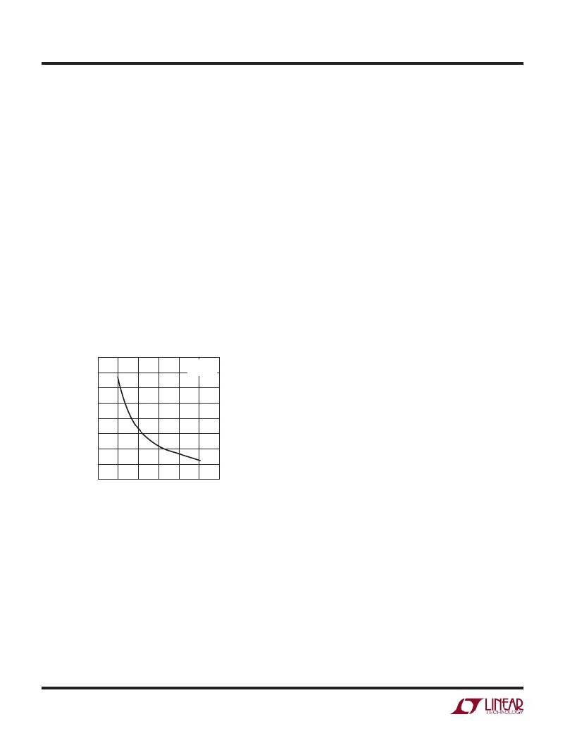
�Operating� Frequency�
�Selection� of� the� operating� frequency� is� a� trade-off� between�
�efficiency� and� component� size.� High� frequency� operation�
�allows� for� smaller� inductor� and� capacitor� values.� Operation�
�at� lower� frequencies� improves� the� efficiency� by� reducing�
�internal� gate� charge� losses� but� requires� larger� inductance�
�values� and/or� capacitance� to� maintain� low� output� ripple�
�voltage.�
�The� operating� frequency,� f� CLK� ,� of� the� LTC3569� is� determined�
�by� an� external� resistor� that� is� connected� between� the� R� T�
�pin� and� ground.� The� value� of� the� resistor� sets� the� ramp�
�current� that� charges� and� discharges� an� internal� timing�
�capacitor� within� the� oscillator.� The� relationship� between�
�oscillator� frequency� and� R� T� is� calculated� by� the� following�
�equation:�
�R� T� =� (5.1855� ?� 10?11)� ?� (f� CLK� )� –1.027�
�Or� may� be� selected� following� the� graph� in� Figure� 4.�
�Minimum� On-Time� And� Duty-Cycle�
�The� maximum� usable� operating� frequency� is� limited� by�
�the� minimum� on-time� and� the� required� duty� cycle.� In� buck�
�regulators,� the� duty� cycle� (DC)� is� the� ratio� of� output� to�
�input� voltage:� DC� =� V� OUT� /V� IN� =� t� ON� /(t� OFF� +� t� ON� ).� At� low� duty�
�cycles,� the� SW� node� is� high� for� a� small� fraction� of� the� total�
�clock� period.� As� this� time� period� approaches� the� speed�
�of� the� gate� drive� circuits� and� the� comparators� internal� to�
�the� LTC3569,� the� dynamic� loop� response� suffers.� To� avoid�
�minimum� on-time� issues� it� is� recommended� to� adjust� the�
�operating� frequency� down� so� as� to� keep� the� minimum�
�duty� cycle� pulse� width� above� 80ns.� Thus,� the� maximum�
�operating� frequency� should� be� selected� such� that� the� duty�
�cycle� does� not� demand� SW� pulse� widths� below� the� mini-�
�mum� on-time.� The� maximum� clock� frequency,� f� CLKMAX� ,�
�is� selected� from� either� the� internal� fixed� frequency� clock,�
�or� a� timing� resistor� at� the� R� T� pin,� or� synchronizing� clock�
�applied� to� the� MODE� pin.� The� minimum� on-time� require-�
�ment� is� met� by� adhering� to� the� following� formula:�
�4.1�
�3.6�
�3.1�
�2.6�
�2.1�
�V� IN� =� 3.6V�
�T� A� =� 25°C�
�f� CLKMAX� =� (V� OUT� /V� IN(MAX)� )/t� MIN-ON�
�For� example,� if� V� OUT� is� 0.8V� and� V� IN� ranges� up� to� 5.5V,�
�the� maximum� clock� frequency� is� limited� to� no� more� than�
�1.8MHz.�
�1.6�
�1.1�
�0.6�
�0.1�
�0� 0.1� 0.2� 0.3� 0.4� 0.5� 0.6�
�R� T� (M� )�
�3569� F04�
�Figure� 4.� f� CLK� vs� R� T�
�The� minimum� frequency� is� limited� by� leakage� and� noise�
�coupling� due� to� the� large� resistance� of� R� T� .�
�If� the� R� T� pin� is� tied� to� SV� IN� the� oscillation� frequency� is�
�fixed� at� 2.25MHz.�
�Keep� excess� capacitance� and� noise� (e.g.,� from� the� SW�
�pins)� away� from� the� R� T� pin.� It� is� recommended� to� remove�
�the� GND� plane� beneath� the� R� T� pin� trace,� and� to� route� the�
�R� T� pin� PCB� trace� away� from� the� SW� pins.�
�Mode� Selection� And� Frequency� Synchronization�
�The� MODE� pin� is� a� multi-purpose� pin� which� provides�
�mode� selection� and� frequency� synchronization.� Connect-�
�ing� this� pin� to� SV� IN� enables� Burst� Mode� operation,� which�
�provides� the� best� low� current� efficiency� at� the� cost� of� a�
�higher� output� voltage� ripple.� When� this� pin� is� connected�
�to� ground,� pulse-skipping� operation� is� selected� which�
�provides� the� lowest� output� voltage� and� current� ripple� at�
�the� cost� of� low� current� efficiency.�
�Synchronize� the� LTC3569� to� an� external� clock� signal� by�
�tying� a� clock� source� to� the� MODE� pin.� Select� the� R� T� pin�
�resistance� so� that� the� internal� oscillator� frequency� is� set�
�to� 20%� lower� than� the� applied� external� clock� frequency� to�
�ensure� adequate� slope� compensation,� since� slope� com-�
�pensation� is� derived� from� the� internal� oscillator.� During�
�synchronization,� the� mode� is� set� to� pulse� skipping.�
�The� external� clock� source� applied� to� the� MODE� pin� requires�
�minimum� low� and� high� pulse� widths� of� about� 100ns.�
�3569fd�
�14�
�相关PDF资料 |
PDF描述 |
|---|---|
| AIAP-03-682-K | INDUCTOR 6800UH 10% .322A |
| RBM43DRYN | CONN EDGECARD 86POS DIP .156 SLD |
| AIAP-03-8R2-K | INDUCTOR 8.2UH 10% 9.89A |
| RBM43DRYH | CONN EDGECARD 86POS DIP .156 SLD |
| AIAP-03-472-K | INDUCTOR 4700UH 10% .39A |
相关代理商/技术参数 |
参数描述 |
|---|---|
| LTC3569EUD#PBF | 功能描述:IC REG BUCK SYNC ADJ TRPL 20QFN RoHS:是 类别:集成电路 (IC) >> PMIC - 稳压器 - DC DC 开关稳压器 系列:- 标准包装:250 系列:- 类型:降压(降压) 输出类型:固定 输出数:1 输出电压:1.2V 输入电压:2.05 V ~ 6 V PWM 型:电压模式 频率 - 开关:2MHz 电流 - 输出:500mA 同步整流器:是 工作温度:-40°C ~ 85°C 安装类型:表面贴装 封装/外壳:6-UFDFN 包装:带卷 (TR) 供应商设备封装:6-SON(1.45x1) 产品目录页面:1032 (CN2011-ZH PDF) 其它名称:296-25628-2 |
| LTC3569EUD#TRPBF | 功能描述:IC REG BUCK SYNC ADJ TRPL 20QFN RoHS:是 类别:集成电路 (IC) >> PMIC - 稳压器 - DC DC 开关稳压器 系列:- 标准包装:2,500 系列:- 类型:降压(降压) 输出类型:固定 输出数:1 输出电压:1.2V,1.5V,1.8V,2.5V 输入电压:2.7 V ~ 20 V PWM 型:- 频率 - 开关:- 电流 - 输出:50mA 同步整流器:是 工作温度:-40°C ~ 125°C 安装类型:表面贴装 封装/外壳:10-TFSOP,10-MSOP(0.118",3.00mm 宽)裸露焊盘 包装:带卷 (TR) 供应商设备封装:10-MSOP 裸露焊盘 |
| LTC3569EUDC#PBF | 功能描述:IC REG BUCK SYNC ADJ TRPL 20QFN RoHS:是 类别:集成电路 (IC) >> PMIC - 稳压器 - DC DC 开关稳压器 系列:- 标准包装:2,500 系列:- 类型:降压(降压) 输出类型:固定 输出数:1 输出电压:1.2V,1.5V,1.8V,2.5V 输入电压:2.7 V ~ 20 V PWM 型:- 频率 - 开关:- 电流 - 输出:50mA 同步整流器:是 工作温度:-40°C ~ 125°C 安装类型:表面贴装 封装/外壳:10-TFSOP,10-MSOP(0.118",3.00mm 宽)裸露焊盘 包装:带卷 (TR) 供应商设备封装:10-MSOP 裸露焊盘 |
| LTC3569EUDC#TRPBF | 功能描述:IC REG BUCK SYNC ADJ TRPL 20QFN RoHS:是 类别:集成电路 (IC) >> PMIC - 稳压器 - DC DC 开关稳压器 系列:- 标准包装:2,500 系列:- 类型:降压(降压) 输出类型:固定 输出数:1 输出电压:1.2V,1.5V,1.8V,2.5V 输入电压:2.7 V ~ 20 V PWM 型:- 频率 - 开关:- 电流 - 输出:50mA 同步整流器:是 工作温度:-40°C ~ 125°C 安装类型:表面贴装 封装/外壳:10-TFSOP,10-MSOP(0.118",3.00mm 宽)裸露焊盘 包装:带卷 (TR) 供应商设备封装:10-MSOP 裸露焊盘 |
| LTC3569EUD-PBF | 制造商:LINER 制造商全称:Linear Technology 功能描述:Triple Buck Regulator With 1.2A and Two 600mA Outputs and Individual Programmable References |
发布紧急采购,3分钟左右您将得到回复。