- 您现在的位置:买卖IC网 > PDF目录14075 > LTC3601EMSE#TRPBF (Linear Technology)IC REG BUCK SYNC ADJ 1.5A 16MSOP PDF资料下载
参数资料
| 型号: | LTC3601EMSE#TRPBF |
| 厂商: | Linear Technology |
| 文件页数: | 12/26页 |
| 文件大小: | 0K |
| 描述: | IC REG BUCK SYNC ADJ 1.5A 16MSOP |
| 标准包装: | 2,500 |
| 类型: | 降压(降压) |
| 输出类型: | 可调式 |
| 输出数: | 1 |
| 输出电压: | 0.5 V ~ 14.52 V |
| 输入电压: | 4 V ~ 15 V |
| PWM 型: | 电流模式,混合 |
| 频率 - 开关: | 800kHz ~ 4MHz |
| 电流 - 输出: | 1.5A |
| 同步整流器: | 是 |
| 工作温度: | -40°C ~ 85°C |
| 安装类型: | 表面贴装 |
| 封装/外壳: | 16-TFSOP(0.118",3.00mm 宽)裸露焊盘 |
| 包装: | 带卷 (TR) |
| 供应商设备封装: | 16-MSOP,裸露焊盘 |
�� �
�
�LTC3601�
�APPLICATIONS� INFORMATION�
�V� OUT� =� 0.6V� 1� +�
�usetypesthathavebeensurgetestedforuseinswitching�
�power� supplies.� Aluminum� electrolytic� capacitors� have�
�signi?cantly� higher� ESR� but� can� be� used� in� cost-sensitive�
�applications� provided� that� consideration� is� given� to� ripple�
�current� ratings� and� long-term� reliability.� Ceramic� capacitors�
�have� excellent� low� ESR� characteristics� and� small� footprints.�
�Their� relatively� low� value� of� bulk� capacitance� may� require�
�multiple� capacitors� in� parallel.�
�Using� Ceramic� Input� and� Output� Capacitors�
�Higher� value,� lower� cost� ceramic� capacitors� are� now�
�available� in� small� case� sizes.� Their� high� voltage� rating�
�and� low� ESR� make� them� ideal� for� switching� regulator�
�applications.� However,� due� to� the� self-resonant� and� high-Q�
�characteristics� of� some� types� of� ceramic� capacitors,� care�
�must� be� taken� when� these� capacitors� are� used� at� the� input�
�and� output.� When� a� ceramic� capacitor� is� used� at� the� input,�
�and� the� power� is� supplied� by� a� wall� adapter� through� long�
�wires,� a� load� step� at� the� output� can� induce� ringing� at� the�
�V� IN� input.� At� best,� this� ringing� can� couple� to� the� output� and�
�be� mistaken� as� loop� instability.� At� worst,� a� sudden� inrush�
�of� current� through� the� long� wires� can� potentially� cause� a�
�voltage� spike� at� V� IN� large� enough� to� damage� the� part.� For�
�a� more� detailed� discussion,� refer� to� Application� Note� 88.�
�When� choosing� the� input� and� output� ceramic� capacitors�
�choose� the� X5R� or� X7R� dielectric� formulations.� These�
�dielectrics� provide� the� best� temperature� and� voltage�
�characteristics� for� a� given� value� and� size.�
�INTV� CC� Regulator� Bypass� Capacitor�
�An� internal� low� dropout� (LDO)� regulator� produces� a�
�3.3V� supply� voltage� used� to� power� much� of� the� internal�
�LTC3601� circuitry� including� the� power� MOSFET� gate�
�drivers.� The� INTV� CC� pin� connects� to� the� output� of� this�
�regulator� and� must� have� a� minimum� of� 1μF� of� decoupling�
�results.� Furthermore,� this� supply� is� intended� only� to� supply�
�additional� DC� load� currents� as� desired� and� not� intended�
�to� regulate� large� transient� or� AC� behavior� this� may� impact�
�LTC3601� operation.�
�Boost� Capacitor�
�The� boost� capacitor,� C� BOOST� ,� is� used� to� create� a� voltage� rail�
�above� the� applied� input� voltage� V� IN� .� Speci?cally,� the� boost�
�capacitor� is� charged� to� a� voltage� equal� to� approximately�
�INTV� CC� each� time� the� bottom� power� MOSFET� is� turned�
�on.� The� charge� on� this� capacitor� is� then� used� to� supply�
�the� required� transient� current� during� the� remainder� of� the�
�switching� cycle.� When� the� top� MOSFET� is� turned� on,� the�
�BOOST� pin� voltage� will� be� equal� to� approximately� V� IN� +�
�3.3V.� For� most� applications� a� 0.1μF� ceramic� capacitor� will�
�provide� adequate� performance.�
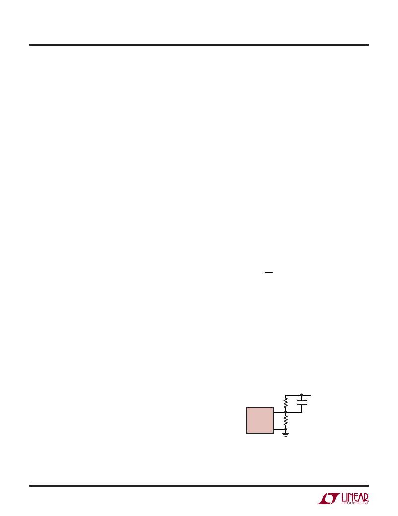
�Output� Voltage� Programming�
�The� LTC3601� will� adjust� the� output� voltage� such� that� V� FB�
�equals� the� reference� voltage� of� 0.6V� according� to:�
�R1�
�R2�
�The� desired� output� voltage� is� set� by� appropriate� selection� of�
�resistors� R1� and� R2� as� shown� in� Figure� 2.� Choosing� large�
�values� for� R1� and� R2� will� result� in� improved� ef?ciency� but�
�may� lead� to� undesirable� noise� coupling� or� phase� margin�
�reduction� due� to� stray� capacitances� at� the� FB� node.� Care�
�should� be� taken� to� route� the� FB� line� away� from� any� noise�
�source,� such� as� the� SW� line.�
�To� improve� the� frequency� response� of� the� main� control�
�loop� a� feedforward� capacitor,� C� F� ,� may� be� used� as� shown�
�in� Figure� 2.�
�V� OUT�
�capacitance� to� ground.� The� decoupling� capacitor� should�
�have� low� impedance� electrical� connections� to� the� INTV� CC�
�FB�
�R1�
�C� F�
�and� PGND� pins� to� provide� the� transient� currents� required�
�LTC3601�
�R2�
�by� the� LTC3601.� The� user� may� connect� a� maximum� load�
�current� of� 5mA� to� this� pin� but� must� take� into� account� the�
�increased� power� dissipation� and� die� temperature� that�
�SGND�
�3601� F02�
�Figure� 2.� Optional� Feedforward� Capacitor�
�3601fb�
�12�
�相关PDF资料 |
PDF描述 |
|---|---|
| HM71-30102LFTR | HIGH PERF LOW COST INDUCTORS |
| HM71-30681LFTR | HIGH PERF LOW COST INDUCTORS |
| LTC3565IDD#TRPBF | IC REG BUCK SYNC ADJ 1.25A 10DFN |
| MAX6869UK21D2L+T | IC MPU SUPERVISOR SOT23-5 |
| HM71-30471LFTR | HIGH PERF LOW COST INDUCTORS |
相关代理商/技术参数 |
参数描述 |
|---|---|
| LTC3601EUD#PBF | 功能描述:IC REG BUCK SYNC ADJ 1.5A 16QFN RoHS:是 类别:集成电路 (IC) >> PMIC - 稳压器 - DC DC 开关稳压器 系列:- 标准包装:250 系列:- 类型:降压(降压) 输出类型:固定 输出数:1 输出电压:1.2V 输入电压:2.05 V ~ 6 V PWM 型:电压模式 频率 - 开关:2MHz 电流 - 输出:500mA 同步整流器:是 工作温度:-40°C ~ 85°C 安装类型:表面贴装 封装/外壳:6-UFDFN 包装:带卷 (TR) 供应商设备封装:6-SON(1.45x1) 产品目录页面:1032 (CN2011-ZH PDF) 其它名称:296-25628-2 |
| LTC3601EUD#TRPBF | 功能描述:IC REG BUCK SYNC ADJ 1.5A 16QFN RoHS:是 类别:集成电路 (IC) >> PMIC - 稳压器 - DC DC 开关稳压器 系列:- 标准包装:2,500 系列:- 类型:升压(升压) 输出类型:可调式 输出数:1 输出电压:1.24 V ~ 30 V 输入电压:1.5 V ~ 12 V PWM 型:电流模式,混合 频率 - 开关:600kHz 电流 - 输出:500mA 同步整流器:无 工作温度:-40°C ~ 85°C 安装类型:表面贴装 封装/外壳:8-SOIC(0.154",3.90mm 宽) 包装:带卷 (TR) 供应商设备封装:8-SOIC |
| LTC3601EUDPBF | 制造商:Linear Technology 功能描述:DC-DC Converter Step-Down 4-15V QFN16EP |
| LTC3601IMSE#PBF | 功能描述:IC REG BUCK SYNC ADJ 1.5A 16MSOP RoHS:是 类别:集成电路 (IC) >> PMIC - 稳压器 - DC DC 开关稳压器 系列:- 标准包装:2,500 系列:- 类型:降压(降压) 输出类型:固定 输出数:1 输出电压:1.2V,1.5V,1.8V,2.5V 输入电压:2.7 V ~ 20 V PWM 型:- 频率 - 开关:- 电流 - 输出:50mA 同步整流器:是 工作温度:-40°C ~ 125°C 安装类型:表面贴装 封装/外壳:10-TFSOP,10-MSOP(0.118",3.00mm 宽)裸露焊盘 包装:带卷 (TR) 供应商设备封装:10-MSOP 裸露焊盘 |
| LTC3601IMSE#TRPBF | 功能描述:IC REG BUCK SYNC ADJ 1.5A 16MSOP RoHS:是 类别:集成电路 (IC) >> PMIC - 稳压器 - DC DC 开关稳压器 系列:- 标准包装:2,500 系列:- 类型:降压(降压) 输出类型:固定 输出数:1 输出电压:1.2V,1.5V,1.8V,2.5V 输入电压:2.7 V ~ 20 V PWM 型:- 频率 - 开关:- 电流 - 输出:50mA 同步整流器:是 工作温度:-40°C ~ 125°C 安装类型:表面贴装 封装/外壳:10-TFSOP,10-MSOP(0.118",3.00mm 宽)裸露焊盘 包装:带卷 (TR) 供应商设备封装:10-MSOP 裸露焊盘 |
发布紧急采购,3分钟左右您将得到回复。