- 您现在的位置:买卖IC网 > PDF目录13932 > LTC3612IUDC#PBF (Linear Technology)IC REG BUCK SYNC ADJ 3A 20QFN PDF资料下载
参数资料
| 型号: | LTC3612IUDC#PBF |
| 厂商: | Linear Technology |
| 文件页数: | 19/30页 |
| 文件大小: | 0K |
| 描述: | IC REG BUCK SYNC ADJ 3A 20QFN |
| 标准包装: | 91 |
| 类型: | 降压(降压) |
| 输出类型: | 可调式 |
| 输出数: | 1 |
| 输出电压: | 0.6 V ~ 5.5 V |
| 输入电压: | 2.25 V ~ 5.5 V |
| PWM 型: | 电流模式,混合 |
| 频率 - 开关: | 300kHz ~ 4MHz |
| 电流 - 输出: | 3A |
| 同步整流器: | 是 |
| 工作温度: | -40°C ~ 125°C |
| 安装类型: | 表面贴装 |
| 封装/外壳: | 20-WFQFN 裸露焊盘 |
| 包装: | 管件 |
| 供应商设备封装: | 20-QFN(3x4) |
第1页第2页第3页第4页第5页第6页第7页第8页第9页第10页第11页第12页第13页第14页第15页第16页第17页第18页当前第19页第20页第21页第22页第23页第24页第25页第26页第27页第28页第29页第30页
�� �
�
�LTC3612�
�APPLICATIONS� INFORMATION�
�AVP� Mode�
�Fast� load� transient� response,� limited� board� space� and� low�
�cost� are� typical� requirements� of� microprocessor� power�
�supplies.� A� microprocessor� has� typical� full� load� step� with�
�very� fast� slew� rate.� The� voltage� at� the� microprocessor� must�
�be� held� to� about� ±0.1V� of� nominal� in� spite� of� these� load�
�current� steps.� Since� the� control� loop� cannot� respond� this�
�fast,� the� output� capacitors� must� supply� the� load� current�
�until� the� control� loop� can� respond.�
�Normally,� several� capacitors� in� parallel� are� required� to�
�meet� microprocessor� transient� requirements.� Capacitor�
�ESR� and� ESL� primarily� determine� the� amount� of� droop� or�
�overshoot� in� the� output� voltage.�
�Consider� the� LTC3612� without� AVP� with� a� bank� of� tantalum�
�output� capacitors.� If� a� load� step� with� very� fast� slew� rate�
�occurs,� the� voltage� excursion� will� be� seen� in� both� direc-�
�tions,� for� full� load� to� minimum� load� transient� and� for� the�
�minimum� load� to� full� load� transient.�
�If� the� ITH� pin� is� tied� to� SV� IN� ,� the� active� voltage� position-�
�ing� (AVP)� mode� and� internal� compensation� are� selected.�
�AVP� mode� intentionally� compromises� load� regulation� by�
�reducing� the� gain� of� the� feedback� circuit,� resulting� in� an�
�output� voltage� that� varies� with� load� current.� When� the� load�
�current� suddenly� increases,� the� output� voltage� starts� from�
�a� level� slightly� higher� than� nominal� so� the� output� voltage�
�can� droop� more� and� stay� within� the� specified� voltage�
�range.� When� the� load� current� suddenly� decreases� the�
�output� voltage� starts� at� a� level� lower� than� nominal� so� the�
�output� voltage� can� have� more� overshoot� and� stay� within�
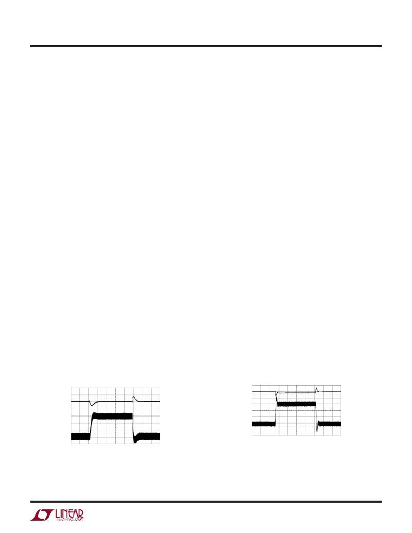
�the� specified� voltage� range� (see� Figures� 3� and� 4).�
�V� OUT�
�200mV/DIV�
�I� L�
�1A/DIV�
�The� benefit� is� a� lower� peak-to-peak� output� voltage� deviation�
�for� a� given� load� step� without� having� to� increase� the� output�
�filter� capacitance.� Alternatively,� the� output� voltage� filter�
�capacitance� can� be� reduced� while� maintaining� the� same�
�peak� to� peak� transient� response.� Due� to� the� reduced� loop�
�gain� in� AVP� mode,� no� external� compensation� is� required.�
�DDR� Mode�
�The� LTC3612� can� both� source� and� sink� current� if� the� MODE�
�pin� is� configured� to� forced� continuous� mode.�
�Current� sinking� is� typically� limited� to� 1.5A,� for� 1MHz�
�frequency� and� a� 1μH� inductor,� but� can� be� lower� at� higher�
�frequencies� and� low� output� voltages.� If� higher� ripple� current�
�can� be� tolerated,� smaller� inductor� values� can� increase� the�
�sink� current� limit.� See� the� Typical� Performance� Charac-�
�teristics� curves� for� more� information.�
�In� addition,� tying� the� DDR� pin� to� SV� IN� ,� lower� external�
�reference� voltage� and� tracking� output� voltage� between�
�channels� are� possible.� See� the� Output� Voltage� Tracking�
�and� External� Reference� Input� sections.�
�Soft-Start�
�The� RUN� pin� provides� a� means� to� shut� down� the� LTC3612.�
�Tying� the� RUN� pin� to� SGND� places� the� LTC3612� in� a� low�
�quiescent� current� shutdown� state� (I� Q� <� 1μA).�
�The� LTC3612� is� enabled� by� pulling� the� RUN� pin� high.� How-�
�ever,� the� applied� voltage� must� not� exceed� SV� IN� .� In� some�
�applications,� the� RUN� signal� is� generated� within� another�
�power� domain� and� is� driven� high� while� the� SV� IN� and� PV� IN�
�is� still� 0V.� In� this� case,� it’s� required� to� limit� the� current� into�
�V� OUT�
�100mV/DIV�
�I� L�
�1A/DIV�
�V� IN� =� 3.3V� 50μs/DIV�
�V� OUT� =� 1.8V�
�I� LOAD� =� 100mA� TO� 3A�
�V� MODE� =� 1.5V�
�COMPENSATION� FIGURE� 1�
�3612� F03�
�V� IN� =� 3.3V� 50μs/DIV�
�V� OUT� =� 1.8V�
�I� LOAD� =� 100mA� TO� 3A�
�V� MODE� =� 1.5V�
�V� ITH� =� 3.3V�
�OUTPUT� CAPACITOR� VALUE� FIGURE� 1�
�3612� F04�
�Figure� 3.� Load� Step� Transient� Forced� Continuous� Mode�
�(AVP� Inactive)�
�Figure� 4.� Load� Step� Transient� Forced� Continuous� Mode�
�with� AVP� Mode�
�3612fb�
�For� more� information� www.linear.com/LTC3612�
�19�
�相关PDF资料 |
PDF描述 |
|---|---|
| RBC13DRAS-S734 | CONN EDGECARD 26POS .100 R/A EXT |
| MAX6795TPYD3+ | IC REG LIN W/SPR VSR 20-TQFN |
| RSC05DRAI-S734 | CONN EDGECARD 10POS .100 R/A PCB |
| MAX6795TPZD4+ | IC REG LIN W/SPR VSR 20-TQFN |
| RMC05DRAI-S734 | CONN EDGECARD 10POS .100 R/A PCB |
相关代理商/技术参数 |
参数描述 |
|---|---|
| LTC3613EWKH#PBF | 功能描述:IC REG BUCK SYNC ADJ 15A 56-QFN RoHS:是 类别:集成电路 (IC) >> PMIC - 稳压器 - DC DC 开关稳压器 系列:- 设计资源:Design Support Tool 标准包装:1 系列:- 类型:升压(升压) 输出类型:固定 输出数:1 输出电压:3V 输入电压:0.75 V ~ 2 V PWM 型:- 频率 - 开关:- 电流 - 输出:100mA 同步整流器:是 工作温度:-40°C ~ 85°C 安装类型:表面贴装 封装/外壳:SOT-23-5 细型,TSOT-23-5 包装:剪切带 (CT) 供应商设备封装:TSOT-23-5 其它名称:AS1323-BTTT-30CT |
| LTC3613EWKH#TRPBF | 功能描述:IC REG BUCK SYNC ADJ 15A 56QFN RoHS:是 类别:集成电路 (IC) >> PMIC - 稳压器 - DC DC 开关稳压器 系列:- 设计资源:Design Support Tool 标准包装:1 系列:- 类型:升压(升压) 输出类型:固定 输出数:1 输出电压:3V 输入电压:0.75 V ~ 2 V PWM 型:- 频率 - 开关:- 电流 - 输出:100mA 同步整流器:是 工作温度:-40°C ~ 85°C 安装类型:表面贴装 封装/外壳:SOT-23-5 细型,TSOT-23-5 包装:剪切带 (CT) 供应商设备封装:TSOT-23-5 其它名称:AS1323-BTTT-30CT |
| LTC3613IWKH#PBF | 功能描述:IC REG BUCK SYNC ADJ 15A 56QFN RoHS:是 类别:集成电路 (IC) >> PMIC - 稳压器 - DC DC 开关稳压器 系列:- 设计资源:Design Support Tool 标准包装:1 系列:- 类型:升压(升压) 输出类型:固定 输出数:1 输出电压:3V 输入电压:0.75 V ~ 2 V PWM 型:- 频率 - 开关:- 电流 - 输出:100mA 同步整流器:是 工作温度:-40°C ~ 85°C 安装类型:表面贴装 封装/外壳:SOT-23-5 细型,TSOT-23-5 包装:剪切带 (CT) 供应商设备封装:TSOT-23-5 其它名称:AS1323-BTTT-30CT |
| LTC3613IWKH#TRPBF | 功能描述:IC REG BUCK SYNC ADJ 15A 56QFN RoHS:是 类别:集成电路 (IC) >> PMIC - 稳压器 - DC DC 开关稳压器 系列:- 设计资源:Design Support Tool 标准包装:1 系列:- 类型:升压(升压) 输出类型:固定 输出数:1 输出电压:3V 输入电压:0.75 V ~ 2 V PWM 型:- 频率 - 开关:- 电流 - 输出:100mA 同步整流器:是 工作温度:-40°C ~ 85°C 安装类型:表面贴装 封装/外壳:SOT-23-5 细型,TSOT-23-5 包装:剪切带 (CT) 供应商设备封装:TSOT-23-5 其它名称:AS1323-BTTT-30CT |
| LTC3614EUDD#PBF | 功能描述:IC REG BUCK SYNC ADJ 4A 24QFN RoHS:是 类别:集成电路 (IC) >> PMIC - 稳压器 - DC DC 开关稳压器 系列:- 标准包装:250 系列:- 类型:降压(降压) 输出类型:固定 输出数:1 输出电压:1.2V 输入电压:2.05 V ~ 6 V PWM 型:电压模式 频率 - 开关:2MHz 电流 - 输出:500mA 同步整流器:是 工作温度:-40°C ~ 85°C 安装类型:表面贴装 封装/外壳:6-UFDFN 包装:带卷 (TR) 供应商设备封装:6-SON(1.45x1) 产品目录页面:1032 (CN2011-ZH PDF) 其它名称:296-25628-2 |
发布紧急采购,3分钟左右您将得到回复。