- 您现在的位置:买卖IC网 > PDF目录13932 > LTC3612IUDC#PBF (Linear Technology)IC REG BUCK SYNC ADJ 3A 20QFN PDF资料下载
参数资料
| 型号: | LTC3612IUDC#PBF |
| 厂商: | Linear Technology |
| 文件页数: | 21/30页 |
| 文件大小: | 0K |
| 描述: | IC REG BUCK SYNC ADJ 3A 20QFN |
| 标准包装: | 91 |
| 类型: | 降压(降压) |
| 输出类型: | 可调式 |
| 输出数: | 1 |
| 输出电压: | 0.6 V ~ 5.5 V |
| 输入电压: | 2.25 V ~ 5.5 V |
| PWM 型: | 电流模式,混合 |
| 频率 - 开关: | 300kHz ~ 4MHz |
| 电流 - 输出: | 3A |
| 同步整流器: | 是 |
| 工作温度: | -40°C ~ 125°C |
| 安装类型: | 表面贴装 |
| 封装/外壳: | 20-WFQFN 裸露焊盘 |
| 包装: | 管件 |
| 供应商设备封装: | 20-QFN(3x4) |
第1页第2页第3页第4页第5页第6页第7页第8页第9页第10页第11页第12页第13页第14页第15页第16页第17页第18页第19页第20页当前第21页第22页第23页第24页第25页第26页第27页第28页第29页第30页
�� �
�
�LTC3612�
�APPLICATIONS� INFORMATION�
�V� OUT2�
�R4�
�R2�
�V� FB2�
�LTC3612�
�TRACK/SS2�
�V� OUT1�
�R4� R3�
�R2� R2�
�R4� ≤� R3�
�V� FB1�
�LTC3612�
�TRACK/SS1�
�V� IN�
�Efficiency� Considerations�
�The� efficiency� of� a� switching� regulator� is� equal� to� the� output�
�power� divided� by� the� input� power� times� 100%.� It� is� often�
�useful� to� analyze� individual� losses� to� determine� what� is�
�limiting� the� efficiency� and� which� change� would� produce�
�the� most� improvement.� Efficiency� can� be� expressed� as:�
�LTC3612� CHANNEL� 2�
�SLAVE�
�LTC3612� CHANNEL� 1�
�MASTER�
�3612� F06a�
�Efficiency� =� 100%� –� (L1� +� L2� +� L3� +� ...)�
�LTC3612�
�LTC3612�
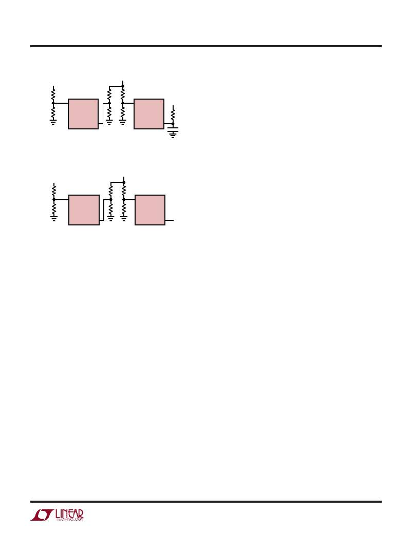
�Figure� 6a.� Set-Up� for� Coincident� Tracking�
�V� OUT1�
�V� OUT2�
�R1� R5� R3� R1/R2� <� R5/R6�
�V� FB2� V� FB1�
�R2� R6� R4�
�TRACK/SS2� TRACK/SS1� V� IN�
�LTC3612� CHANNEL� 2� LTC3612� CHANNEL� 1�
�SLAVE� MASTER� 3612� F06b�
�Figure� 6b.� Set-Up� for� Ratiometric� Tracking�
�For� coincident� start-up,� the� voltage� value� at� the� TRACK/SS�
�pin� for� the� slave� channel� needs� to� reach� the� final� reference�
�value� after� the� internal� soft-start� time� (around� 1ms).� The�
�master� start-up� time� needs� to� be� adjusted� with� an� external�
�capacitor� and� resistor� to� ensure� this.�
�External� Reference� Input� (DDR� Mode)�
�If� the� DDR� pin� is� tied� to� SV� IN� (DDR� mode),� the� run� state� is�
�entered� when� V� TRACK/SS� exceeds� 0.3V� and� tracking� down�
�behavior� is� possible� if� the� V� TRACK/SS� voltage� is� below� 0.6V.�
�This� allows� TRACK/SS� to� be� used� as� an� external� reference�
�between� 0.3V� and� 0.6V� if� desired.� During� the� run� state� in�
�DDR� mode,� the� power� good� window� moves� in� relation�
�to� the� actual� TRACK/SS� pin� voltage� if� the� voltage� value�
�is� between� 0.3V� and� 0.6V.� Note:� if� TRACK/SS� voltage� is�
�0.6V,� either� the� tracking� circuit� or� the� internal� reference�
�can� be� used.�
�During� up/down� tracking� the� output� current� foldback� is�
�disabled� and� the� PGOOD� pin� is� always� pulled� down� (see�
�Figure� 8).�
�where� L1,� L2,� etc.� are� the� individual� losses� as� a� percent-�
�age� of� input� power.�
�Although� all� dissipative� elements� in� the� circuit� produce�
�losses,� two� main� sources� usually� account� for� most� of�
�the� losses:� V� IN� quiescent� current� and� I� 2� R� losses.� The� V� IN�
�quiescent� current� loss� dominates� the� efficiency� loss� at�
�very� low� load� currents� whereas� the� I� 2� R� loss� dominates�
�the� efficiency� loss� at� medium� to� high� load� currents.� In� a�
�typical� efficiency� plot,� the� efficiency� curve� at� very� low� load�
�currents� can� be� misleading� since� the� actual� power� lost� is�
�usually� of� no� consequence.�
�1.� The� V� IN� quiescent� current� is� due� to� two� components:� the�
�DC� bias� current� as� given� in� the� Electrical� Characteristics�
�and� the� internal� main� switch� and� synchronous� switch�
�gate� charge� currents.� The� gate� charge� current� results�
�from� switching� the� gate� capacitance� of� the� internal� power�
�MOSFET� switches.� Each� time� the� gate� is� switched� from�
�low� to� high� to� low� again,� a� packet� of� charge� dQ� moves�
�from� V� IN� to� ground.� The� resulting� dQ/dt� is� the� current�
�out� of� V� IN� due� to� gate� charge,� and� it� is� typically� larger�
�than� the� DC� bias� current.� Both� the� DC� bias� and� gate�
�charge� losses� are� proportional� to� V� IN� ;� thus,� their� effects�
�will� be� more� pronounced� at� higher� supply� voltages.�
�2.� I� 2� R� losses� are� calculated� from� the� resistances� of� the�
�internal� switches,� R� SW� ,� and� external� inductor,� R� L� .� In�
�continuous� mode� the� average� output� current� flowing�
�through� inductor� L� is� “chopped”� between� the� main�
�switch� and� the� synchronous� switch.� Thus,� the� series�
�resistance� looking� into� the� SW� pin� is� a� function� of� both�
�top� and� bottom� MOSFET� R� DS(ON)� and� the� duty� cycle�
�(DC)� as� follows:�
�R� SW� =� (R� DS(ON)TOP� )(DC)� +� (R� DS(ON)BOT� )(1� –� DC)�
�3612fb�
�For� more� information� www.linear.com/LTC3612�
�21�
�相关PDF资料 |
PDF描述 |
|---|---|
| RBC13DRAS-S734 | CONN EDGECARD 26POS .100 R/A EXT |
| MAX6795TPYD3+ | IC REG LIN W/SPR VSR 20-TQFN |
| RSC05DRAI-S734 | CONN EDGECARD 10POS .100 R/A PCB |
| MAX6795TPZD4+ | IC REG LIN W/SPR VSR 20-TQFN |
| RMC05DRAI-S734 | CONN EDGECARD 10POS .100 R/A PCB |
相关代理商/技术参数 |
参数描述 |
|---|---|
| LTC3613EWKH#PBF | 功能描述:IC REG BUCK SYNC ADJ 15A 56-QFN RoHS:是 类别:集成电路 (IC) >> PMIC - 稳压器 - DC DC 开关稳压器 系列:- 设计资源:Design Support Tool 标准包装:1 系列:- 类型:升压(升压) 输出类型:固定 输出数:1 输出电压:3V 输入电压:0.75 V ~ 2 V PWM 型:- 频率 - 开关:- 电流 - 输出:100mA 同步整流器:是 工作温度:-40°C ~ 85°C 安装类型:表面贴装 封装/外壳:SOT-23-5 细型,TSOT-23-5 包装:剪切带 (CT) 供应商设备封装:TSOT-23-5 其它名称:AS1323-BTTT-30CT |
| LTC3613EWKH#TRPBF | 功能描述:IC REG BUCK SYNC ADJ 15A 56QFN RoHS:是 类别:集成电路 (IC) >> PMIC - 稳压器 - DC DC 开关稳压器 系列:- 设计资源:Design Support Tool 标准包装:1 系列:- 类型:升压(升压) 输出类型:固定 输出数:1 输出电压:3V 输入电压:0.75 V ~ 2 V PWM 型:- 频率 - 开关:- 电流 - 输出:100mA 同步整流器:是 工作温度:-40°C ~ 85°C 安装类型:表面贴装 封装/外壳:SOT-23-5 细型,TSOT-23-5 包装:剪切带 (CT) 供应商设备封装:TSOT-23-5 其它名称:AS1323-BTTT-30CT |
| LTC3613IWKH#PBF | 功能描述:IC REG BUCK SYNC ADJ 15A 56QFN RoHS:是 类别:集成电路 (IC) >> PMIC - 稳压器 - DC DC 开关稳压器 系列:- 设计资源:Design Support Tool 标准包装:1 系列:- 类型:升压(升压) 输出类型:固定 输出数:1 输出电压:3V 输入电压:0.75 V ~ 2 V PWM 型:- 频率 - 开关:- 电流 - 输出:100mA 同步整流器:是 工作温度:-40°C ~ 85°C 安装类型:表面贴装 封装/外壳:SOT-23-5 细型,TSOT-23-5 包装:剪切带 (CT) 供应商设备封装:TSOT-23-5 其它名称:AS1323-BTTT-30CT |
| LTC3613IWKH#TRPBF | 功能描述:IC REG BUCK SYNC ADJ 15A 56QFN RoHS:是 类别:集成电路 (IC) >> PMIC - 稳压器 - DC DC 开关稳压器 系列:- 设计资源:Design Support Tool 标准包装:1 系列:- 类型:升压(升压) 输出类型:固定 输出数:1 输出电压:3V 输入电压:0.75 V ~ 2 V PWM 型:- 频率 - 开关:- 电流 - 输出:100mA 同步整流器:是 工作温度:-40°C ~ 85°C 安装类型:表面贴装 封装/外壳:SOT-23-5 细型,TSOT-23-5 包装:剪切带 (CT) 供应商设备封装:TSOT-23-5 其它名称:AS1323-BTTT-30CT |
| LTC3614EUDD#PBF | 功能描述:IC REG BUCK SYNC ADJ 4A 24QFN RoHS:是 类别:集成电路 (IC) >> PMIC - 稳压器 - DC DC 开关稳压器 系列:- 标准包装:250 系列:- 类型:降压(降压) 输出类型:固定 输出数:1 输出电压:1.2V 输入电压:2.05 V ~ 6 V PWM 型:电压模式 频率 - 开关:2MHz 电流 - 输出:500mA 同步整流器:是 工作温度:-40°C ~ 85°C 安装类型:表面贴装 封装/外壳:6-UFDFN 包装:带卷 (TR) 供应商设备封装:6-SON(1.45x1) 产品目录页面:1032 (CN2011-ZH PDF) 其它名称:296-25628-2 |
发布紧急采购,3分钟左右您将得到回复。