- 您现在的位置:买卖IC网 > PDF目录15342 > LTC3704EMS#TR (Linear Technology)IC REG CTRLR INV PWM CM 10-MSOP PDF资料下载
参数资料
| 型号: | LTC3704EMS#TR |
| 厂商: | Linear Technology |
| 文件页数: | 8/28页 |
| 文件大小: | 0K |
| 描述: | IC REG CTRLR INV PWM CM 10-MSOP |
| 标准包装: | 2,500 |
| PWM 型: | 电流模式 |
| 输出数: | 1 |
| 频率 - 最大: | 1MHz |
| 占空比: | 97% |
| 电源电压: | 2.5 V ~ 36 V |
| 降压: | 无 |
| 升压: | 无 |
| 回扫: | 无 |
| 反相: | 是 |
| 倍增器: | 无 |
| 除法器: | 无 |
| Cuk: | 无 |
| 隔离: | 无 |
| 工作温度: | -40°C ~ 85°C |
| 封装/外壳: | 10-TFSOP,10-MSOP(0.118",3.00mm 宽) |
| 包装: | 带卷 (TR) |
| 其它名称: | LTC3704EMSTR |
第1页第2页第3页第4页第5页第6页第7页当前第8页第9页第10页第11页第12页第13页第14页第15页第16页第17页第18页第19页第20页第21页第22页第23页第24页第25页第26页第27页第28页
�� �
�
�LTC3704�
�OPERATIO�
�Main� Control� Loop�
�The� LTC3704� is� a� constant� frequency,� current� mode�
�controller� for� DC/DC� positive-to-negative� converter� appli-�
�cations.� The� LTC3704� is� distinguished� from� conventional�
�current� mode� controllers� because� the� current� control� loop�
�can� be� closed� by� sensing� the� voltage� drop� across� the�
�power� MOSFET� switch� instead� of� across� a� discrete� sense�
�resistor,� as� shown� in� Figure� 2.� This� sensing� technique�
�improves� efficiency,� increases� power� density,� and� re-�
�duces� the� cost� of� the� overall� solution.�
�The� nominal� operating� frequency� of� the� LTC3704� is� pro-�
�grammed� using� a� resistor� from� the� FREQ� pin� to� ground�
�and� can� be� controlled� over� a� 50kHz� to� 1000kHz� range.� In�
�addition,� the� internal� oscillator� can� be� synchronized� to� an�
�external� clock� applied� to� the� MODE/SYNC� pin� and� can� be�
�locked� to� a� frequency� between� 100%� and� 130%� of� its�
�nominal� value.� When� the� MODE/SYNC� pin� is� left� open,� it� is�
�pulled� low� by� an� internal� 50k� resistor� and� Burst� Mode�
�operation� is� enabled.� If� this� pin� is� taken� above� 2V� or� an�
�external� clock� is� applied,� Burst� Mode� operation� is� disabled�
�and� the� IC� operates� in� continuous� mode.� With� no� load� (or�
�an� extremely� light� load),� the� controller� will� skip� pulses� in�
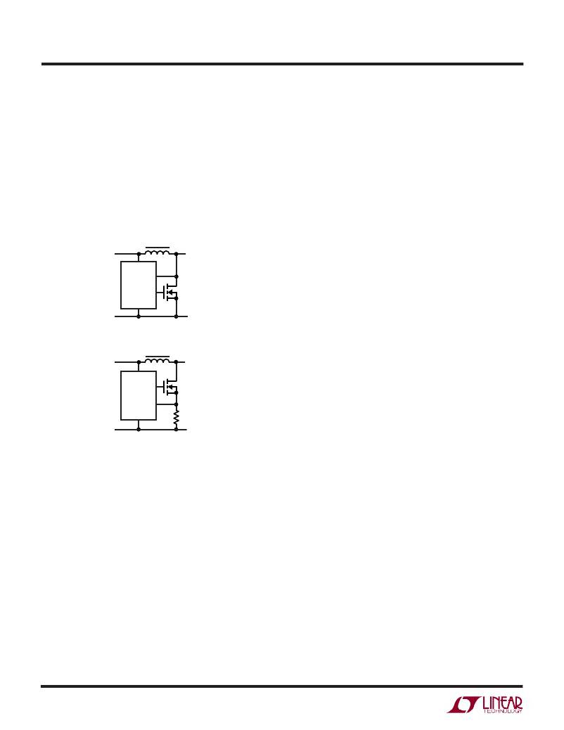
�V� IN�
�V� SW�
�order� to� maintain� regulation� and� prevent� excessive� output�
�V� IN�
�SENSE�
�GATE�
�GND�
�GND�
�2a.� SENSE� Pin� Connection� for�
�Maximum� Efficiency� (V� SW� <� 36V)�
�ripple.�
�The� RUN� pin� controls� whether� the� IC� is� enabled� or� is� in� a�
�low� current� shutdown� state.� A� micropower� 1.248V� refer-�
�ence� and� comparator� C2� allow� the� user� to� program� the�
�supply� voltage� at� which� the� IC� turns� on� and� off� (compara-�
�tor� C2� has� 100mV� of� hysteresis� for� noise� immunity).� With�
�V� IN�
�V� SW�
�the� RUN� pin� below� 1.248V,� the� chip� is� off� and� the� input�
�supply� current� is� typically� only� 10� μ� A.�
�R� SENSE�
�GND�
�V� IN�
�GATE�
�SENSE�
�GND�
�3704� F02�
�2b.� SENSE� Pin� Connection� for� Precise�
�Control� of� Peak� I� IN� /I� OUT� or� for� V� SW� >� 36V�
�Figure� 2.� Using� the� SENSE� Pin� On� the� LTC3704�
�For� circuit� operation,� please� refer� to� the� Block� Diagram� of�
�the� IC� and� Figure� 1.� In� normal� operation,� the� power�
�MOSFET� is� turned� on� when� the� oscillator� sets� the� PWM�
�latch� and� is� turned� off� when� the� current� comparator� C1�
�resets� the� latch.� The� divided-down� output� voltage� is� com-�
�pared� to� an� internal� 1.230V� reference� by� the� error� amplifier�
�EA,� which� outputs� an� error� signal� at� the� I� TH� pin.� The� voltage�
�on� the� I� TH� pin� sets� the� current� comparator� C1� input�
�threshold.� When� the� load� current� increases,� a� fall� in� the�
�NFB� voltage� relative� to� the� reference� voltage� causes� the� I� TH�
�pin� to� rise,� which� causes� the� current� comparator� C1� to� trip�
�at� a� higher� peak� inductor� current� value.� The� average�
�inductor� current� will� therefore� rise� until� it� equals� the� load�
�current,� thereby� maintaining� output� regulation.�
�The� LTC3704� can� be� used� either� by� sensing� the� voltage�
�drop� across� the� power� MOSFET� or� by� connecting� the�
�SENSE� pin� to� a� conventional� shunt� resistor� in� the� source�
�of� the� power� MOSFET,� as� shown� in� Figure� 2.� Sensing� the�
�voltage� across� the� power� MOSFET� maximizes� converter�
�efficiency� and� minimizes� the� component� count,� but� limits�
�the� output� voltage� to� the� maximum� rating� for� this� pin�
�(36V).� By� connecting� the� SENSE� pin� to� a� resistor� in� the�
�source� of� the� power� MOSFET,� the� user� is� able� to� program�
�output� voltages� significantly� greater� than� the� 36V� maxi-�
�mum� input� voltage� rating� for� the� IC.�
�Programming� the� Operating� Mode�
�For� applications� where� maximizing� the� efficiency� at� very�
�light� loads� (e.g.,� <100� μ� A)� is� a� high� priority,� Burst� Mode�
�operation� should� be� applied� (i.e.,� the� MODE/SYNC� pin�
�should� be� connected� to� ground).� In� applications� where�
�fixed� frequency� operation� is� more� critical� than� low� cur-�
�rent� efficiency,� or� where� the� lowest� output� ripple� is�
�desired,� pulse-skip� mode� operation� should� be� used� and�
�the� MODE/SYNC� pin� should� be� connected� to� the� INTV� CC�
�pin.� This� allows� discontinuous� conduction� mode� (DCM)�
�operation� down� to� near� the� limit� defined� by� the� chip’s�
�3704fb�
�8�
�相关PDF资料 |
PDF描述 |
|---|---|
| RSC17DRTI | CONN EDGECARD 34POS DIP .100 SLD |
| ADM8698ANZ | IC SUPERVISOR MPU 4.65V 8DIP |
| EBC17DREF-S734 | CONN EDGECARD 34POS .100 EYELET |
| GCC31DCST-S288 | CONN EDGECARD 62POS .100 EXTEND |
| VE-BWV-EV-F3 | CONVERTER MOD DC/DC 5.8V 150W |
相关代理商/技术参数 |
参数描述 |
|---|---|
| LTC3704IMS | 制造商:Linear Technology 功能描述:DC DC Cntrlr Single-OUT Pos-Neg 2.5V to 36V Input 10-Pin MSOP |
| LTC3704IMS#PBF | 功能描述:IC REG CTRLR INV PWM CM 10-MSOP RoHS:是 类别:集成电路 (IC) >> PMIC - 稳压器 - DC DC 切换控制器 系列:- 标准包装:2,500 系列:- PWM 型:电流模式 输出数:1 频率 - 最大:500kHz 占空比:96% 电源电压:4 V ~ 36 V 降压:无 升压:是 回扫:无 反相:无 倍增器:无 除法器:无 Cuk:无 隔离:无 工作温度:-40°C ~ 125°C 封装/外壳:24-WQFN 裸露焊盘 包装:带卷 (TR) |
| LTC3704IMS#TR | 制造商:Linear Technology 功能描述:DC DC Cntrlr Single-OUT Pos-Neg 2.5V to 36V Input 10-Pin MSOP T/R |
| LTC3704IMS#TRPBF | 功能描述:IC REG CTRLR INV PWM CM 10-MSOP RoHS:是 类别:集成电路 (IC) >> PMIC - 稳压器 - DC DC 切换控制器 系列:- 标准包装:2,500 系列:- PWM 型:电流模式 输出数:1 频率 - 最大:500kHz 占空比:96% 电源电压:4 V ~ 36 V 降压:无 升压:是 回扫:无 反相:无 倍增器:无 除法器:无 Cuk:无 隔离:无 工作温度:-40°C ~ 125°C 封装/外壳:24-WQFN 裸露焊盘 包装:带卷 (TR) |
| LTC3705EGN#PBF | 功能描述:IC CTRLR OCP 16SSOP RoHS:是 类别:集成电路 (IC) >> PMIC - AC-DC 转换器,离线开关 系列:- 标准包装:3,000 系列:- 输出隔离:隔离 频率范围:61kHz ~ 71kHz 输入电压:9.4 V ~ 28 V 输出电压:12V 功率(瓦特):- 工作温度:-40°C ~ 125°C 封装/外壳:SC-74,SOT-457 供应商设备封装:6-TSOP 包装:带卷 (TR) |
发布紧急采购,3分钟左右您将得到回复。