- 您现在的位置:买卖IC网 > PDF目录1831 > LTC3721EGN-1#PBF (Linear Technology)IC REG CTRLR ISO PWM CM 16-SSOP PDF资料下载
参数资料
| 型号: | LTC3721EGN-1#PBF |
| 厂商: | Linear Technology |
| 文件页数: | 9/16页 |
| 文件大小: | 0K |
| 描述: | IC REG CTRLR ISO PWM CM 16-SSOP |
| 标准包装: | 100 |
| PWM 型: | 电流模式 |
| 输出数: | 1 |
| 频率 - 最大: | 1MHz |
| 占空比: | 50% |
| 电源电压: | 10V(最小值) |
| 降压: | 无 |
| 升压: | 无 |
| 回扫: | 无 |
| 反相: | 无 |
| 倍增器: | 无 |
| 除法器: | 无 |
| Cuk: | 无 |
| 隔离: | 是 |
| 工作温度: | -40°C ~ 85°C |
| 封装/外壳: | 16-SSOP(0.154",3.90mm 宽) |
| 包装: | 管件 |
| 产品目录页面: | 1335 (CN2011-ZH PDF) |
�� �
�
�LTC3721-1�
�OPERATIO�
�Please� refer� to� the� detailed� Block� Diagram� for� this� discus-�
�sion.� The� LTC3721-1� is� a� PWM� push-pull� controller� that�
�operates� with� pulse-by-pulse� peak� current� mode� control.�
�It� is� best� suited� for� moderate� to� high� power� isolated� power�
�systems� where� small� size� and� high� efficiency� are� required.�
�The� push-pull� topology� delivers� excellent� transformer�
�utilization� and� requires� only� two� low� side� power� MOSFET�
�switches.� The� controller� generates� 180� °� out� of� phase�
�0%� to� <� 50%� duty� cycle� drive� signals� on� DRVA� and� DRVB.�
�The� external� MOSFETs� are� driven� directly� by� these� power-�
�sets� a� maximum� deadtime� if� DPRG� is� floated.� The� internal�
�current� source� causes� the� programmed� deadtime� to� vary�
�non-linearly� with� increasing� values� of� R� DPRG� (see� Typical�
�Performance� Characteristics).� An� external� 200k� resistor�
�connected� from� DPRG� to� GND� will� compensate� for� the�
�internal� 10� μ� A� current� source� and� linearize� the� deadtime�
�delay� vs� R� DPRG� characteristic.�
�V� REF�
�ful� on-chip� drivers.� The� external� MOSFETs� typically� con-�
�R� DPRG�
�DPRG�
�trol� opposite� primary� windings� of� a� centertapped� power�
�transformer.� The� centertap� primary� winding� is� connected�
�to� the� input� DC� feed.� The� secondary� of� the� transformer� can�
�be� configured� in� different� synchronous� or� nonsynchronous�
�configurations� depending� on� the� application� needs.�
�OPTIONAL�
�200k�
�+�
�V� 2V�
�–�
�2.5V�
�+�
�–�
�TURN-ON�
�OUTPUT�
�37211� F01�
�The� duty� ratio� is� controlled� by� the� voltage� on� COMP.� A�
�switching� cycle� commences� with� the� falling� edge� of� the�
�internal� oscillator� clock� pulse.� The� LTC3721-1� attenuates�
�the� voltage� on� COMP� and� compares� it� to� the� current� sense�
�signal� to� terminate� the� switching� cycle.� If� the� voltage� on� CS�
�exceeds� 300mV,� the� present� cycle� is� terminated.� If� the�
�voltage� on� CS� exceeds� 600mV,� all� switching� stops� and� a�
�soft-start� sequence� is� initiated.�
�A� host� of� other� features� including� an� error� amplifier,�
�system� UVLO� programming,� adjustable� leading� edge� blank-�
�ing,� slope� compensation� and� programmable� dead-time�
�provide� flexibility� for� a� variety� of� applications.�
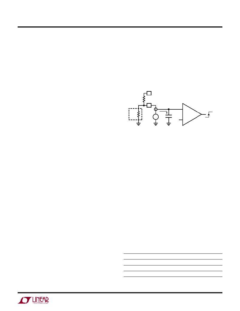
�Programming� Driver� Dead-Time�
�The� LTC3721-1� includes� a� feature� to� program� the� mini-�
�mum� time� between� the� output� signals� on� DRVA� and� DRVB�
�commonly� referred� to� as� the� driver� dead-time.� This� func-�
�tion� will� come� into� play� if� the� controller� is� commanded� for�
�maximum� duty� cycle.� The� dead-time� is� set� with� an�
�external� resistor� connected� between� DPRG� and� V� REF� (see�
�Figure� 1).� The� nominal� regulated� voltage� on� DPRG� is� 2V.�
�Figure� 1.� Deadtime� Adjust�
�Powering� the� LTC3721-1�
�The� LTC3721-1� utilizes� an� integrated� V� CC� shunt� regulator�
�to� serve� the� dual� purposes� of� limiting� the� voltage� applied�
�to� V� CC� as� well� as� signaling� that� the� chip’s� bias� voltage� is�
�sufficient� to� begin� switching� operation� (under� voltage�
�lockout).� With� its� typical� 10.2V� turn-on� voltage� and� 4.2V�
�UVLO� hysteresis,� the� LTC3721-1� is� tolerant� of� loosely�
�regulated� input� sources� such� as� an� auxiliary� transformer�
�winding.� The� V� CC� shunt� is� capable� of� sinking� up� to� 40mA�
�of� externally� applied� current.� The� UVLO� turn-on� and� turn-�
�off� thresholds� are� derived� from� an� internally� trimmed�
�reference� making� them� extremely� accurate.� In� addition,�
�the� LTC3721-1� exhibits� very� low� (145� μ� A� typ)� start-up�
�current� that� allows� the� use� of� 1/8W� to� 1/4W� trickle� charge�
�start-up� resistors.�
�The� trickle� charge� resistor� should� be� selected� as� follows:�
�R� START(MAX)� =� V� IN(MIN)� –� 10.7V/250� μ� A�
�Adding� a� small� safety� margin� and� choosing� standard�
�values� yields:�
�The� external� resistor� programs� a� current� which� flows� into�
�DPRG.� The� dead-time� can� be� adjusted� from� 90ns� to� 300ns�
�with� this� resistor.� The� dead-time� can� also� be� modulated�
�based� on� an� external� current� source� that� feeds� current� into�
�DPRG.� Care� must� be� taken� to� limit� the� current� fed� into�
�APPLICATION�
�DC/DC�
�Off-Line�
�PFC� Preregulator�
�V� IN� RANGE�
�36V� to� 72V�
�85V� to� 270V� RMS�
�390V� DC�
�R� START�
�100k�
�430k�
�1.4M�
�DPRG� to� 350� μ� A� or� less.� An� internal� 10� μ� A� current� source�
�sn37211� 37211fs�
�9�
�相关PDF资料 |
PDF描述 |
|---|---|
| LTC3722EGN-2#TRPBF | IC REG CTRLR DIV ISO PWM 24SSOP |
| LTC3723EGN-1#PBF | IC REG CTRLR FLYBK ISO CM 16SSOP |
| LTC3727EUH-1#PBF | IC REG CTRLR BUCK PWM CM 32-QFN |
| LTC3728EUH#PBF | IC REG CTRLR BUCK PWM CM 32-QFN |
| LTC3729EUH#PBF | IC REG CTRLR BUCK PWM CM 32-QFN |
相关代理商/技术参数 |
参数描述 |
|---|---|
| LTC3721EUF-1 | 功能描述:IC REG CTRLR ISO PWM CM 16-QFN RoHS:否 类别:集成电路 (IC) >> PMIC - 稳压器 - DC DC 切换控制器 系列:- 标准包装:4,500 系列:PowerWise® PWM 型:控制器 输出数:1 频率 - 最大:1MHz 占空比:95% 电源电压:2.8 V ~ 5.5 V 降压:是 升压:无 回扫:无 反相:无 倍增器:无 除法器:无 Cuk:无 隔离:无 工作温度:-40°C ~ 125°C 封装/外壳:6-WDFN 裸露焊盘 包装:带卷 (TR) 配用:LM1771EVAL-ND - BOARD EVALUATION LM1771 其它名称:LM1771SSDX |
| LTC3721EUF-1#PBF | 功能描述:IC REG CTRLR ISO PWM CM 16-QFN RoHS:是 类别:集成电路 (IC) >> PMIC - 稳压器 - DC DC 切换控制器 系列:- 标准包装:4,500 系列:PowerWise® PWM 型:控制器 输出数:1 频率 - 最大:1MHz 占空比:95% 电源电压:2.8 V ~ 5.5 V 降压:是 升压:无 回扫:无 反相:无 倍增器:无 除法器:无 Cuk:无 隔离:无 工作温度:-40°C ~ 125°C 封装/外壳:6-WDFN 裸露焊盘 包装:带卷 (TR) 配用:LM1771EVAL-ND - BOARD EVALUATION LM1771 其它名称:LM1771SSDX |
| LTC3721EUF-1#TR | 功能描述:IC REG CTRLR ISO PWM CM 16-QFN RoHS:否 类别:集成电路 (IC) >> PMIC - 稳压器 - DC DC 切换控制器 系列:- 标准包装:4,500 系列:PowerWise® PWM 型:控制器 输出数:1 频率 - 最大:1MHz 占空比:95% 电源电压:2.8 V ~ 5.5 V 降压:是 升压:无 回扫:无 反相:无 倍增器:无 除法器:无 Cuk:无 隔离:无 工作温度:-40°C ~ 125°C 封装/外壳:6-WDFN 裸露焊盘 包装:带卷 (TR) 配用:LM1771EVAL-ND - BOARD EVALUATION LM1771 其它名称:LM1771SSDX |
| LTC3721EUF-1#TRPBF | 功能描述:IC REG CTRLR ISO PWM CM 16-QFN RoHS:是 类别:集成电路 (IC) >> PMIC - 稳压器 - DC DC 切换控制器 系列:- 标准包装:4,500 系列:PowerWise® PWM 型:控制器 输出数:1 频率 - 最大:1MHz 占空比:95% 电源电压:2.8 V ~ 5.5 V 降压:是 升压:无 回扫:无 反相:无 倍增器:无 除法器:无 Cuk:无 隔离:无 工作温度:-40°C ~ 125°C 封装/外壳:6-WDFN 裸露焊盘 包装:带卷 (TR) 配用:LM1771EVAL-ND - BOARD EVALUATION LM1771 其它名称:LM1771SSDX |
| LTC3722EGN-1 | 功能描述:IC REG CTRLR DIV ISO PWM 24SSOP RoHS:否 类别:集成电路 (IC) >> PMIC - 稳压器 - DC DC 切换控制器 系列:- 标准包装:4,500 系列:PowerWise® PWM 型:控制器 输出数:1 频率 - 最大:1MHz 占空比:95% 电源电压:2.8 V ~ 5.5 V 降压:是 升压:无 回扫:无 反相:无 倍增器:无 除法器:无 Cuk:无 隔离:无 工作温度:-40°C ~ 125°C 封装/外壳:6-WDFN 裸露焊盘 包装:带卷 (TR) 配用:LM1771EVAL-ND - BOARD EVALUATION LM1771 其它名称:LM1771SSDX |
发布紧急采购,3分钟左右您将得到回复。