- 您现在的位置:买卖IC网 > PDF目录15286 > LTC3732CUHF#PBF (Linear Technology)IC REG CTRLR BUCK PWM CM 38-QFN PDF资料下载
参数资料
| 型号: | LTC3732CUHF#PBF |
| 厂商: | Linear Technology |
| 文件页数: | 14/28页 |
| 文件大小: | 0K |
| 描述: | IC REG CTRLR BUCK PWM CM 38-QFN |
| 标准包装: | 52 |
| PWM 型: | 电流模式 |
| 输出数: | 1 |
| 频率 - 最大: | 750kHz |
| 占空比: | 98.5% |
| 电源电压: | 4.5 V ~ 7 V |
| 降压: | 是 |
| 升压: | 无 |
| 回扫: | 无 |
| 反相: | 无 |
| 倍增器: | 无 |
| 除法器: | 无 |
| Cuk: | 无 |
| 隔离: | 无 |
| 工作温度: | 0°C ~ 70°C |
| 封装/外壳: | 38-WFQFN 裸露焊盘 |
| 包装: | 管件 |
第1页第2页第3页第4页第5页第6页第7页第8页第9页第10页第11页第12页第13页当前第14页第15页第16页第17页第18页第19页第20页第21页第22页第23页第24页第25页第26页第27页第28页
�� �
�
�LTC3732�
�APPLICATIO� S� I� FOR� ATIO�
�?� I�
�?�
�(� )�
�P� MAIN� =� OUT� ?� MAX� ?� 1� +� δ� R� DS� (� ON� )� +�
�(� )(� )�
�V� IN�
�R� DR� C� MILLER� ?�
�()�
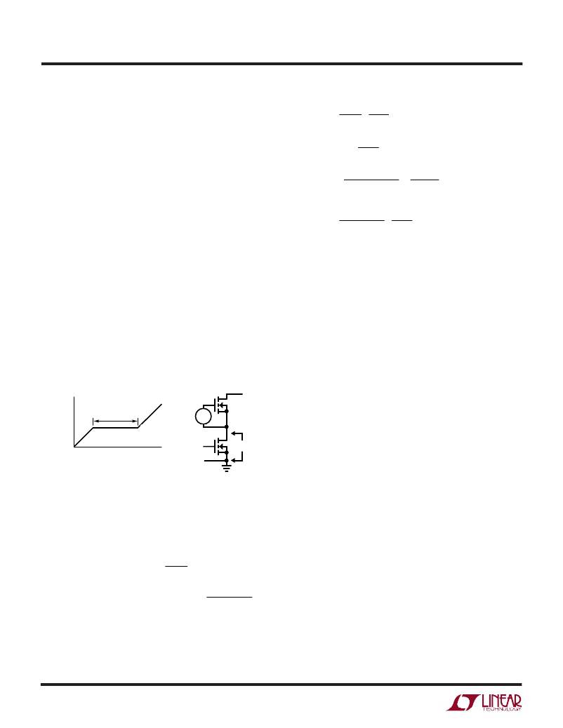
�Thecurveisgeneratedbyforcingaconstantinputcurrent�
�into� the� gate� of� a� common� source,� current� source� loaded�
�stage� and� then� plotting� the� gate� voltage� versus� time.� The�
�initial� slope� is� the� effect� of� the� gate-to-source� and� the� gate-�
�to-drain� capacitance.� The� flat� portion� of� the� curve� is� the�
�result� of� the� Miller� multiplication� effect� of� the� drain-to-gate�
�capacitance� as� the� drain� drops� the� voltage� across� the�
�current� source� load.� The� upper� sloping� line� is� due� to� the�
�2�
�V�
�V� IN� ?� N� ?�
�2� I� MAX�
�2� N�
�?� 1� 1� ?�
�?� ?�
�?� V� CC� –� V� TH� (� IL� )� V� TH� (� IL� )� ?�
�?� +� ?� f�
�?� I�
�?�
�(� )�
�=� IN� OUT� ?� MAX� ?� 1� +� δ� R� DS� (� ON� )�
�drain-to-gate accumulation capacitance and the gate-to-�
�source� capacitance.� The� Miller� charge� (the� increase� in�
�coulombs� on� the� horizontal� axis� from� a� to� b� while� the� curve�
�P� SYNC�
�V� –� V�
�V� IN� ?� N� ?�
�2�
�is� flat)� is� specified� for� a� given� V� DS� drain� voltage,� but� can� be�
�adjusted� for� different� V� DS� voltages� by� multiplying� by� the�
�ratio� of� the� application� V� DS� to� the� curve� specified� V� DS�
�values.� A� way� to� estimate� the� C� MILLER� term� is� to� take� the�
�change� in� gate� charge� from� points� a� and� b� on� a� manufac-�
�turers� data� sheet� and� divide� by� the� stated� V� DS� voltage�
�specified.� C� MILLER� is� the� most� important� selection� criteria�
�for� determining� the� transition� loss� term� in� the� top� MOSFET�
�but� is� not� directly� specified� on� MOSFET� data� sheets.� C� RSS�
�and� C� OS� are� specified� sometimes� but� definitions� of� these�
�parameters� are� not� included.�
�V� IN�
�where� N� is� the� number� of� output� stages,� δ� is� the� tempera-�
�ture� dependency� of� R� DS(ON)� ,� R� DR� is� the� effective� top� driver�
�resistance� (approximately� 2� ?� at� V� GS� =� V� MILLER� ),� V� IN� is� the�
�drain� potential� and� the� change� in� drain� potential� in� the�
�particular� application.� V� TH(IL)� is� the� data� sheet� specified�
�typical� gate� threshold� voltage� specified� in� the� power�
�MOSFET� data� sheet� at� the� specified� drain� current.� C� MILLER�
�is� the� calculated� capacitance� using� the� gate� charge� curve�
�from� the� MOSFET� data� sheet� and� the� technique� described�
�above.�
�Both� MOSFETs� have� I� 2� R� losses� while� the� topside� N-channel�
�equation� includes� an� additional� term� for� transition� losses,�
�V� GS�
�MILLER� EFFECT�
�V�
�which� peak� at� the� highest� input� voltage.� For� V� IN� <� 12V,� the�
�a� b�
�Q� IN�
�C� MILLER� =� (Q� B� –� Q� A� )/V� DS�
�+�
�V� GS�
�–�
�+� V� DS�
�–�
�3732� F05�
�high� current� efficiency� generally� improves� with� larger�
�MOSFETs,� while� for� V� IN� >� 12V,� the� transition� losses�
�rapidly� increase� to� the� point� that� the� use� of� a� higher�
�R� DS(ON)� device� with� lower� C� MILLER� actually� provides� higher�
�Main� Switch� Duty� Cycle� =�
�Synchronous� Switch� Duty� Cycle� =� ?� IN� OUT� ?�
�Figure 5. Gate Charge Characteristic�
�When� the� controller� is� operating� in� continuous� mode� the�
�duty� cycles� for� the� top� and� bottom� MOSFETs� are� given� by:�
�V� OUT�
�V� IN�
�?� V� –� V� ?�
�?� V� IN� ?�
�The� power� dissipation� for� the� main� and� synchronous�
�MOSFETs� at� maximum� output� current� are� given� by:�
�efficiency.� The� synchronous� MOSFET� losses� are� greatest�
�at� high� input� voltage� when� the� top� switch� duty� factor� is� low�
�or� during� a� short� circuit� when� the� synchronous� switch� is�
�on� close� to� 100%� of� the� period.�
�The� term� (1� +� δ� )� is� generally� given� for� a� MOSFET� in� the�
�form� of� a� normalized� R� DS(ON)� vs� temperature� curve,� but�
�δ� =� 0.005/� °� C� can� be� used� as� an� approximation� for� low�
�voltage� MOSFETs.�
�The� Schottky� diodes,� D1� to� D3� shown� in� Figure� 1� conduct�
�during� the� dead� time� between� the� conduction� of� the� two�
�large� power� MOSFETs.� This� prevents� the� body� diode� of� the�
�bottom� MOSFET� from� turning� on,� storing� charge� during�
�the� dead� time� and� requiring� a� reverse� recovery� period�
�which� could� cost� as� much� as� several� percent� in� efficiency.�
�3732f�
�14�
�相关PDF资料 |
PDF描述 |
|---|---|
| LTC1735IGN#TR | IC REG CTRLR BUCK PWM CM 16-SSOP |
| VI-B2Z-EY-F4 | CONVERTER MOD DC/DC 2V 20W |
| LTC3810HUH-5#TRPBF | IC REG CTRLR BUCK PWM CM 32-QFN |
| LTC3834EUFD#TRPBF | IC REG CTRLR BUCK PWM CM 20-QFN |
| LTC3834EFE#TRPBF | IC REG CTRLR BUCK PWM CM 20TSSOP |
相关代理商/技术参数 |
参数描述 |
|---|---|
| LTC3733CG | 功能描述:IC CTRLR BUCK AMD 3PHASE 36-SSOP RoHS:否 类别:集成电路 (IC) >> PMIC - 稳压器 - 专用型 系列:- 标准包装:43 系列:- 应用:控制器,Intel VR11 输入电压:5 V ~ 12 V 输出数:1 输出电压:0.5 V ~ 1.6 V 工作温度:-40°C ~ 85°C 安装类型:表面贴装 封装/外壳:48-VFQFN 裸露焊盘 供应商设备封装:48-QFN(7x7) 包装:管件 |
| LTC3733CG#PBF | 功能描述:IC CTRLR BUCK AMD 3PHASE 36-SSOP RoHS:是 类别:集成电路 (IC) >> PMIC - 稳压器 - 专用型 系列:- 标准包装:43 系列:- 应用:控制器,Intel VR11 输入电压:5 V ~ 12 V 输出数:1 输出电压:0.5 V ~ 1.6 V 工作温度:-40°C ~ 85°C 安装类型:表面贴装 封装/外壳:48-VFQFN 裸露焊盘 供应商设备封装:48-QFN(7x7) 包装:管件 |
| LTC3733CG#TR | 功能描述:IC CTRLR BUCK 3PH AMD CPU 36SSOP RoHS:否 类别:集成电路 (IC) >> PMIC - 稳压器 - 专用型 系列:- 标准包装:43 系列:- 应用:控制器,Intel VR11 输入电压:5 V ~ 12 V 输出数:1 输出电压:0.5 V ~ 1.6 V 工作温度:-40°C ~ 85°C 安装类型:表面贴装 封装/外壳:48-VFQFN 裸露焊盘 供应商设备封装:48-QFN(7x7) 包装:管件 |
| LTC3733CG#TRPBF | 功能描述:IC CTRLR BUCK AMD 3PHASE 36-SSOP RoHS:是 类别:集成电路 (IC) >> PMIC - 稳压器 - 专用型 系列:- 标准包装:43 系列:- 应用:控制器,Intel VR11 输入电压:5 V ~ 12 V 输出数:1 输出电压:0.5 V ~ 1.6 V 工作温度:-40°C ~ 85°C 安装类型:表面贴装 封装/外壳:48-VFQFN 裸露焊盘 供应商设备封装:48-QFN(7x7) 包装:管件 |
| LTC3733CUHF-1 | 功能描述:IC CTRLR BUCK 3PH AMD CPU 38-QFN RoHS:否 类别:集成电路 (IC) >> PMIC - 稳压器 - 专用型 系列:- 标准包装:43 系列:- 应用:控制器,Intel VR11 输入电压:5 V ~ 12 V 输出数:1 输出电压:0.5 V ~ 1.6 V 工作温度:-40°C ~ 85°C 安装类型:表面贴装 封装/外壳:48-VFQFN 裸露焊盘 供应商设备封装:48-QFN(7x7) 包装:管件 |
发布紧急采购,3分钟左右您将得到回复。