- 您现在的位置:买卖IC网 > PDF目录69007 > LTC3736-2EGN#PBF (LINEAR TECHNOLOGY CORP) SWITCHING CONTROLLER, PDSO24 PDF资料下载
参数资料
| 型号: | LTC3736-2EGN#PBF |
| 厂商: | LINEAR TECHNOLOGY CORP |
| 元件分类: | 稳压器 |
| 英文描述: | SWITCHING CONTROLLER, PDSO24 |
| 封装: | 0.150 INCH, LEAD FREE, PLASTIC, SSOP-24 |
| 文件页数: | 16/28页 |
| 文件大小: | 344K |
| 代理商: | LTC3736-2EGN#PBF |
第1页第2页第3页第4页第5页第6页第7页第8页第9页第10页第11页第12页第13页第14页第15页当前第16页第17页第18页第19页第20页第21页第22页第23页第24页第25页第26页第27页第28页
LTC3736-2
23
37362fb
APPLICATIONS INFORMATION
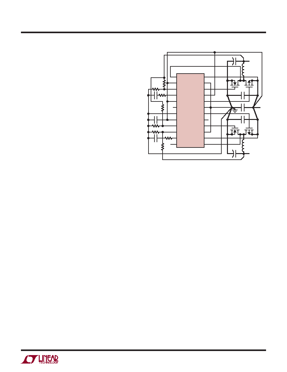
Figures 13. LTC3736-2 Layout Diagram
related to the stability of the closed-loop system and will
demonstrate the actual overall supply performance. For
a detailed explanation of optimizing the compensation
components, including a review of control loop theory,
refer to Application Note 76.
A second, more severe transient is caused by switching
in loads with large (>1μF) supply bypass capacitors. The
discharged bypass capacitors are effectively put in parallel
with COUT, causing a rapid drop in VOUT. No regulator can
deliver enough current to prevent this problem if the load
switch resistance is low and it is driven quickly. The only
solution is to limit the rise time of the switch drive so that
the load rise time is limited to approximately (25)(CLOAD).
Thus a 10μF capacitor would require a 250μs rise time,
limiting the charging current to about 200mA.
PC Board Layout Checklist
When laying out the printed circuit board, the following
checklist should be used to ensure proper operation of
the LTC3736-2. These items are illustrated in the layout
diagram of Figure 13. Figure 14 depicts the current wave-
forms present in the various branches of the 2-phase dual
regulator.
1. The power loop (input capacitor, MOSFETs, inductor,
output capacitor) of each channel should be as small
as possible and isolated as much as possible from the
power loop of the other channel. Ideally, the drains of
the P- and N-channel FETs should be connected close
to one another with an input capacitor placed across
the FET sources (from the P-channel source to the N-
channel source) right at the FETs. It is better to have
two separate, smaller valued input capacitors (e.g., two
10μF—one for each channel) than it is to have a single
larger valued capacitor (e.g., 22μF) that the channels
share with a common connection.
2. The signal and power grounds should be kept separate.
The signal ground consists of the feedback resistor divid-
ers, ITH compensation networks and the SGND pin.
The power grounds consist of the (–) terminal of the
input and output capacitors and the source of the N-
channel MOSFET. Each channel should have its own
power ground for its power loop (as described above
in item 1). The power grounds for the two channels
should connect together at a common point. It is most
important to keep the ground paths with high switching
currents away from each other.
The PGND pins on the LTC3736-2 IC should be shorted
together and connected to the common power ground
connection (away from the switching currents).
3. Put the feedback resistors close to the VFB pins. The
trace connecting the top feedback resistor (RB) to
the output capacitor should be a Kelvin trace. The ITH
compensation components should also be very close
to the LTC3736-2.
4. The current sense traces (SENSE+ and SW) should
be Kelvin connections right at the P-channel MOSFET
source and drain.
5. Keep the switch nodes (SW1, SW2) and the gate driver
nodes (TG1, TG2, BG1, BG2) away from the small-signal
components, especially the opposite channel’s feedback
resistors, ITH compensation components, and the cur-
rent sense pins (SENSE+ and SW).
SW1
IPRG1
VFB1
ITH1
IPRG2
PLLLPF
SGND
VIN
TRACK
VFB2
ITH2
PGOOD
SENSE1+
PGND
BG1
SYNC/FCB
TG1
PGND
TG2
RUN/SS
BG2
PGND
SENSE2+
SW2
1
2
3
4
5
6
7
8
9
10
11
12
24
23
22
21
20
19
18
17
16
15
14
13
LTC3736EGN-2
+
COUT1
COUT2
CVIN1
CVIN
VOUT1
VOUT2
BOLD LINES INDICATE HIGH CURRENT PATHS
37362 F13
L1
L2
MN1
MP1
MN2
MP2
VIN
CVIN2
相关PDF资料 |
PDF描述 |
|---|---|
| LTC3785EUF-1#TRPBF | 3 A SWITCHING REGULATOR, 650 kHz SWITCHING FREQ-MAX, PQCC24 |
| LTC3785EUF-1#PBF | 3 A SWITCHING REGULATOR, 650 kHz SWITCHING FREQ-MAX, PQCC24 |
| LTC3823EUH | 4 A SWITCHING CONTROLLER, 200 kHz SWITCHING FREQ-MAX, PQCC32 |
| LTC3823EGN | 4 A SWITCHING CONTROLLER, 200 kHz SWITCHING FREQ-MAX, PDSO28 |
| LTC3823EUH#TR | 4 A SWITCHING CONTROLLER, 200 kHz SWITCHING FREQ-MAX, PQCC32 |
相关代理商/技术参数 |
参数描述 |
|---|---|
| LTC3736EGN | 功能描述:IC REG CTRLR BUCK PWM CM 24-SSOP RoHS:否 类别:集成电路 (IC) >> PMIC - 稳压器 - DC DC 切换控制器 系列:PolyPhase® 标准包装:2,500 系列:- PWM 型:电流模式 输出数:1 频率 - 最大:500kHz 占空比:96% 电源电压:4 V ~ 36 V 降压:无 升压:是 回扫:无 反相:无 倍增器:无 除法器:无 Cuk:无 隔离:无 工作温度:-40°C ~ 125°C 封装/外壳:24-WQFN 裸露焊盘 包装:带卷 (TR) |
| LTC3736EGN#PBF | 功能描述:IC REG CTRLR BUCK PWM CM 24-SSOP RoHS:是 类别:集成电路 (IC) >> PMIC - 稳压器 - DC DC 切换控制器 系列:PolyPhase® 特色产品:LM3753/54 Scalable 2-Phase Synchronous Buck Controllers 标准包装:1 系列:PowerWise® PWM 型:电压模式 输出数:1 频率 - 最大:1MHz 占空比:81% 电源电压:4.5 V ~ 18 V 降压:是 升压:无 回扫:无 反相:无 倍增器:无 除法器:无 Cuk:无 隔离:无 工作温度:-5°C ~ 125°C 封装/外壳:32-WFQFN 裸露焊盘 包装:Digi-Reel® 产品目录页面:1303 (CN2011-ZH PDF) 其它名称:LM3754SQDKR |
| LTC3736EGN#TR | 功能描述:IC REG CTRLR BUCK PWM CM 24-SSOP RoHS:否 类别:集成电路 (IC) >> PMIC - 稳压器 - DC DC 切换控制器 系列:PolyPhase® 标准包装:2,500 系列:- PWM 型:电流模式 输出数:1 频率 - 最大:500kHz 占空比:96% 电源电压:4 V ~ 36 V 降压:无 升压:是 回扫:无 反相:无 倍增器:无 除法器:无 Cuk:无 隔离:无 工作温度:-40°C ~ 125°C 封装/外壳:24-WQFN 裸露焊盘 包装:带卷 (TR) |
| LTC3736EGN#TRPBF | 功能描述:IC REG CTRLR BUCK PWM CM 24-SSOP RoHS:是 类别:集成电路 (IC) >> PMIC - 稳压器 - DC DC 切换控制器 系列:PolyPhase® 标准包装:2,500 系列:- PWM 型:电流模式 输出数:1 频率 - 最大:500kHz 占空比:96% 电源电压:4 V ~ 36 V 降压:无 升压:是 回扫:无 反相:无 倍增器:无 除法器:无 Cuk:无 隔离:无 工作温度:-40°C ~ 125°C 封装/外壳:24-WQFN 裸露焊盘 包装:带卷 (TR) |
| LTC3736EGN-1 | 功能描述:IC REG CTRLR BUCK PWM CM 24-SSOP RoHS:否 类别:集成电路 (IC) >> PMIC - 稳压器 - DC DC 切换控制器 系列:PolyPhase® 标准包装:4,500 系列:PowerWise® PWM 型:控制器 输出数:1 频率 - 最大:1MHz 占空比:95% 电源电压:2.8 V ~ 5.5 V 降压:是 升压:无 回扫:无 反相:无 倍增器:无 除法器:无 Cuk:无 隔离:无 工作温度:-40°C ~ 125°C 封装/外壳:6-WDFN 裸露焊盘 包装:带卷 (TR) 配用:LM1771EVAL-ND - BOARD EVALUATION LM1771 其它名称:LM1771SSDX |
发布紧急采购,3分钟左右您将得到回复。