参数资料
| 型号: | LTC3786EUD#PBF |
| 厂商: | Linear Technology |
| 文件页数: | 18/34页 |
| 文件大小: | 0K |
| 描述: | IC REG CTRLR BST PWM CM 16-QFN |
| 标准包装: | 121 |
| PWM 型: | 电流模式 |
| 输出数: | 1 |
| 频率 - 最大: | 850kHz |
| 占空比: | 100% |
| 电源电压: | 4.5 V ~ 38 V |
| 降压: | 无 |
| 升压: | 是 |
| 回扫: | 无 |
| 反相: | 无 |
| 倍增器: | 无 |
| 除法器: | 无 |
| Cuk: | 无 |
| 隔离: | 无 |
| 工作温度: | -40°C ~ 125°C |
| 封装/外壳: | 16-WFQFN 裸露焊盘 |
| 包装: | 管件 |
第1页第2页第3页第4页第5页第6页第7页第8页第9页第10页第11页第12页第13页第14页第15页第16页第17页当前第18页第19页第20页第21页第22页第23页第24页第25页第26页第27页第28页第29页第30页第31页第32页第33页第34页
�� �
�
�LTC3786�
�APPLICATIONS� INFORMATION�
�t� SS� =� C� SS� ?�
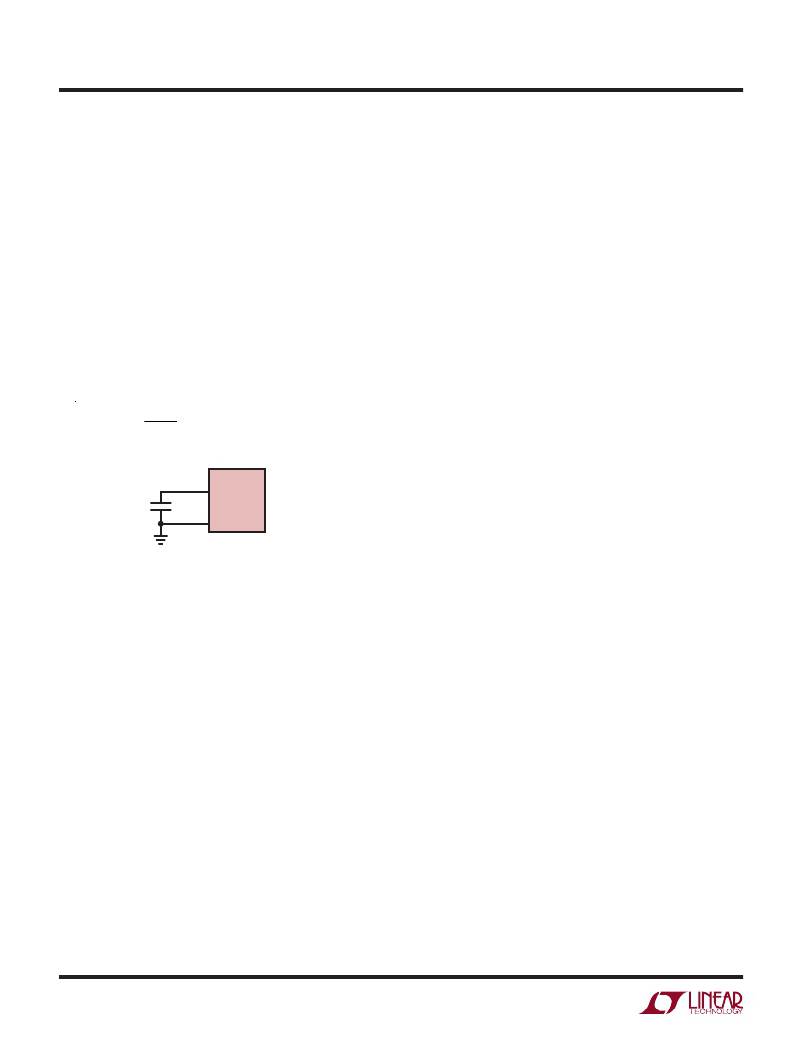
�Soft-Start(SSPin)�
�The� start-up� of� the� V� OUT� is� controlled� by� the� voltage� on�
�the� SS� pin.� When� the� voltage� on� the� SS� pin� is� less� than�
�the� internal� 1.2V� reference,� the� LTC3786� regulates� the� VFB�
�pin� voltage� to� the� voltage� on� the� SS� pin� instead� of� 1.2V.�
�Soft-start� is� enabled� by� simply� connecting� a� capacitor� from�
�the� SS� pin� to� ground,� as� shown� in� Figure� 4.� An� internal�
�10μA� current� source� charges� the� capacitor,� providing� a�
�linear� ramping� voltage� at� the� SS� pin.� The� LTC3786� will�
�regulate� the� V� FB� pin� (and� hence,� V� OUT� )� according� to� the�
�voltage� on� the� SS� pin,� allowing� V� OUT� to� rise� smoothly�
�from� V� IN� to� its� final� regulated� value.� The� total� soft-start�
�time� will� be� approximately:�
�1.2V�
�10μA�
�LTC3786�
�SS�
�C� SS�
�SGND�
�3786� F04�
�Figure� 4.� Using� the� SS� Pin� to� Program� Soft-Start�
�INTV� CC� Regulator�
�The� LTC3786� features� an� internal� P-channel� low� dropout�
�linear� regulator� (LDO)� that� supplies� power� at� the� INTV� CC�
�pin� from� the� VBIAS� supply� pin.� INTV� CC� powers� the� gate�
�drivers� and� much� of� the� LTC3786’s� internal� circuitry.� The�
�VBIAS� LDO� regulates� INTV� CC� to� 5.4V.� It� can� supply� at� least�
�50mA� and� must� be� bypassed� to� ground� with� a� minimum�
�of� 4.7μF� ceramic� capacitor.� Good� bypassing� is� needed� to�
�supply� the� high� transient� currents� required� by� the� MOSFET�
�gate� drivers.�
�High� input� voltage� applications� in� which� large� MOSFETs�
�are� being� driven� at� high� frequencies� may� cause� the�
�maximum� junction� temperature� rating� for� the� LTC3786�
�to� be� exceeded.� The� power� dissipation� for� the� IC� is� equal�
�to� VBIAS� ?� I� INTVCC� .� The� gate� charge� current� is� dependent�
�on� operating� frequency,� as� discussed� in� the� Efficiency�
�Considerations� section.� The� junction� temperature� can� be�
�estimated� by� using� the� equations� given� in� Note� 2� of� the�
�Electrical� Characteristics.� For� example,� at� 70°C� ambient�
�temperature,� the� LTC3786� INTV� CC� current� is� limited� to�
�less� than� 20mA� in� the� QFN� package� from� a� 40V� supply:�
�T� J� =� 70°C� +� (20mA)(40V)(68°C/W)� =� 125°C�
�In� an� MSOP� package,� the� INTV� CC� current� is� limited� to� less�
�than� 34mA� from� a� 40V� supply:�
�T� J� =� 70°C� +� (34mA)(40V)(40°C/W)� =� 125°C�
�To� prevent� the� maximum� junction� temperature� from� being�
�exceeded,� the� input� supply� current� must� be� checked� while�
�operating� in� continuous� conduction� mode� (PLLIN/MODE�
�=� INTV� CC� )� at� maximum� VBIAS.�
�Topside� MOSFET� Driver� Supply� (C� B� ,� D� B� )�
�External� bootstrap� capacitors,� C� B� ,� connected� to� the�
�BOOST� pin� supplies� the� gate� drive� voltage� for� the� topside�
�MOSFET.� Capacitor� C� B� in� the� Block� Diagram� is� charged�
�though� external� diode,� D� B� ,� from� INTV� CC� when� the� SW� pin�
�is� low.� When� the� topside� MOSFET� is� to� be� turned� on,� the�
�driver� places� the� C� B� voltage� across� the� gate-source� of� the�
�desired� MOSFET.� This� enhances� the� MOSFET� and� turns� on�
�the� topside� switch.� The� switch� node� voltage,� SW,� rises� to�
�V� OUT� and� the� BOOST� pin� follows.� With� the� topside� MOSFET�
�on,� the� boost� voltage� is� above� the� output� voltage:� V� BOOST�
�=� V� OUT� +� V� INTVCC� .� The� value� of� the� boost� capacitor,� C� B� ,�
�needs� to� be� 100� times� that� of� the� total� input� capacitance�
�of� the� topside� MOSFET(s).� The� reverse� breakdown� of� the�
�external� Schottky� diode� must� be� greater� than� V� IN(MAX)� .�
�The� external� diode� D� B� can� be� a� Schottky� diode� or� silicon�
�diode,� but� in� either� case� it� should� have� low� leakage� and� fast�
�recovery.� Pay� close� attention� to� the� reverse� leakage� at� high�
�temperatures� where� it� generally� increases� substantially.�
�The� topside� MOSFET� driver� includes� an� internal� charge�
�pump� that� delivers� current� to� the� bootstrap� capacitor� from�
�the� BOOST� pin.� This� charge� current� maintains� the� bias�
�voltage� required� to� keep� the� top� MOSFET� on� continuously�
�during� dropout/overvoltage� conditions.� The� Schottky/�
�silicon� diode� selected� for� the� topside� driver� should� have� a�
�reverse� leakage� less� than� the� available� output� current� the�
�charge� pump� can� supply.� Curves� displaying� the� available�
�charge� pump� current� under� different� operating� conditions�
�can� be� found� in� the� Typical� Performance� Characteristics�
�section.�
�3786fa�
�18�
�相关PDF资料 |
PDF描述 |
|---|---|
| LTC3787EUFD#PBF | IC REG CTRLR BST PWM CM 28-QFN |
| LTC3788IUH#TRPBF | IC REG CTRLR BST PWM CM 32-QFN |
| LTC3789EGN#PBF | IC REG CTRLR BST PWM CM 28-SSOP |
| LTC3801BES6#TRM | IC REG CTRLR BUCK PWM TSOT23-6 |
| LTC3802EGN | IC REG CTRLR BUCK PWM VM 28-SSOP |
相关代理商/技术参数 |
参数描述 |
|---|---|
| LTC3786IMSE#PBF | 功能描述:IC REG CTRLR BST PWM CM 16-MSOP RoHS:是 类别:集成电路 (IC) >> PMIC - 稳压器 - DC DC 切换控制器 系列:- 标准包装:2,500 系列:- PWM 型:电流模式 输出数:1 频率 - 最大:500kHz 占空比:96% 电源电压:4 V ~ 36 V 降压:无 升压:是 回扫:无 反相:无 倍增器:无 除法器:无 Cuk:无 隔离:无 工作温度:-40°C ~ 125°C 封装/外壳:24-WQFN 裸露焊盘 包装:带卷 (TR) |
| LTC3786IMSE#TRPBF | 功能描述:IC REG CTRLR BST PWM CM 16-MSOP RoHS:是 类别:集成电路 (IC) >> PMIC - 稳压器 - DC DC 切换控制器 系列:- 标准包装:2,500 系列:- PWM 型:电流模式 输出数:1 频率 - 最大:500kHz 占空比:96% 电源电压:4 V ~ 36 V 降压:无 升压:是 回扫:无 反相:无 倍增器:无 除法器:无 Cuk:无 隔离:无 工作温度:-40°C ~ 125°C 封装/外壳:24-WQFN 裸露焊盘 包装:带卷 (TR) |
| LTC3786IUD#PBF | 功能描述:IC REG CTRLR BST PWM CM 16-QFN RoHS:是 类别:集成电路 (IC) >> PMIC - 稳压器 - DC DC 切换控制器 系列:- 标准包装:2,500 系列:- PWM 型:电流模式 输出数:1 频率 - 最大:500kHz 占空比:96% 电源电压:4 V ~ 36 V 降压:无 升压:是 回扫:无 反相:无 倍增器:无 除法器:无 Cuk:无 隔离:无 工作温度:-40°C ~ 125°C 封装/外壳:24-WQFN 裸露焊盘 包装:带卷 (TR) |
| LTC3786IUD#TRPBF | 功能描述:IC REG CTRLR BST PWM CM 16-QFN RoHS:是 类别:集成电路 (IC) >> PMIC - 稳压器 - DC DC 切换控制器 系列:- 标准包装:2,500 系列:- PWM 型:电流模式 输出数:1 频率 - 最大:500kHz 占空比:96% 电源电压:4 V ~ 36 V 降压:无 升压:是 回扫:无 反相:无 倍增器:无 除法器:无 Cuk:无 隔离:无 工作温度:-40°C ~ 125°C 封装/外壳:24-WQFN 裸露焊盘 包装:带卷 (TR) |
| LTC3787EGN#PBF | 功能描述:IC REG CTRLR BST PWM CM 28-SSOP RoHS:是 类别:集成电路 (IC) >> PMIC - 稳压器 - DC DC 切换控制器 系列:PolyPhase® 特色产品:LM3753/54 Scalable 2-Phase Synchronous Buck Controllers 标准包装:1 系列:PowerWise® PWM 型:电压模式 输出数:1 频率 - 最大:1MHz 占空比:81% 电源电压:4.5 V ~ 18 V 降压:是 升压:无 回扫:无 反相:无 倍增器:无 除法器:无 Cuk:无 隔离:无 工作温度:-5°C ~ 125°C 封装/外壳:32-WFQFN 裸露焊盘 包装:Digi-Reel® 产品目录页面:1303 (CN2011-ZH PDF) 其它名称:LM3754SQDKR |
发布紧急采购,3分钟左右您将得到回复。