- 您现在的位置:买卖IC网 > PDF目录1832 > LTC3806EDE#TRPBF (Linear Technology)IC REG CTRLR FLYBACK PWM 12-DFN PDF资料下载
参数资料
| 型号: | LTC3806EDE#TRPBF |
| 厂商: | Linear Technology |
| 文件页数: | 15/20页 |
| 文件大小: | 0K |
| 描述: | IC REG CTRLR FLYBACK PWM 12-DFN |
| 标准包装: | 2,500 |
| PWM 型: | 电流模式 |
| 输出数: | 1 |
| 频率 - 最大: | 290kHz |
| 占空比: | 94% |
| 电源电压: | 10 V ~ 75 V |
| 降压: | 无 |
| 升压: | 无 |
| 回扫: | 是 |
| 反相: | 无 |
| 倍增器: | 无 |
| 除法器: | 无 |
| Cuk: | 无 |
| 隔离: | 无 |
| 工作温度: | -40°C ~ 85°C |
| 封装/外壳: | 12-WFDFN 裸露焊盘 |
| 包装: | 带卷 (TR) |
�� �
�
�LTC3806�
�APPLICATIO� S� I� FOR� ATIO�
�Continuing� our� previous� example� the� filter� capacitor� for�
�output� 1� needs:�
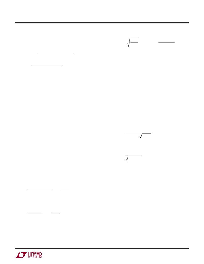
�BV� DSS� ≥� I� PK�
�L� LKG�
�C� P�
�+� V� IN� (� MAX� )� +�
�V� OUT� (� MAX� )�
�N�
�ESR� COUT� ≤�
�0.01? 3 .3 V ?� (� 1– 0 .579� )�
�2� A�
�=� 7� m� Ω�
�where� L� LKG� is� the� primary-side� leakage� inductance� and� C� P�
�is� the� primary-side� capacitance� (mostly� from� the� C� OSS� of�
�C� OUT� ≥�
�2� A�
�0� .� 0� 1� ?� 3� .� 3� V� ?� 250� kHz�
�=� 242� μ� F�
�the� primary-side� power� MOSFET).� A� snubber� may� be�
�added� to� reduce� the� leakage� inductance� related� spike.� For�
�more� information� on� snubber� design,� refer� to� Application�
�To� get� an� electrolytic� capcitor� with� an� ESR� this� low� would�
�require� C� OUT� much� larger� than� 242� μ� F.� Combining� a� low�
�ESR� ceramic� capacitor� in� parallel� with� an� electrolytic�
�capacitor� provides� better� filtering� at� lower� cost.�
�For� output� 2,� the� output� capacitor� needs� an� ESR� less� than�
�42m� Ω� and� a� bulk� C� greater� than� 40.4� μ� F.� This� can� be�
�achieved� with� a� single� high� performance� capacitor� such� as�
�a� Sanyo� OS-CON� or� equivalent.�
�Once� the� output� capacitor� ESR� and� bulk� capacitance� have�
�been� determined,� the� overall� ripple� voltage� waveform�
�Note� 19.�
�For� each� secondary-side� power� MOSFET,� the� BV� DSS� should�
�be� greater� than:�
�BV� DSS� ≥� V� OUT� +� V� IN(MAX)� ?� N�
�Next,� select� a� logic-level� MOSFET� with� acceptable� R� DS(ON)�
�at� the� nominal� gate� drive� voltage� (usually� 6.9V—set� by� the�
�INTV� CC� regulator).�
�Calculate� the� required� RMS� currents� next.� For� the� primary-�
�side� power� MOSFET:�
�should� be� verified� on� a� dedicated� PC� board.� Parasitic�
�inductance� from� poor� layout� can� have� a� significant� impact�
�on� ripple.� Refer� to� the� layout� section� for� details.�
�I� RMSPRI� =�
�P� IN�
�V� IN� (� MIN� )� ?� D� MAX�
�Power� MOSFET� Selection�
�For� each� secondary-side� power� MOSFET:�
�Important� selection� criteria� for� the� power� MOSFETs� in-�
�clude� the� “on”� resistance� R� DS(ON)� ,� input� capacitance,�
�drain-to-source� breakdown� voltage� (BV� DSS� )� and� maxi-�
�I� RMSSEC� =�
�I� OUT�
�1� ?� D� MAX�
�mum� drain� current� (I� D(MAX)� ).�
�Narrow� the� choices� for� power� MOSFETs� by� first� looking� at�
�the� maximum� drain� currents.� For� the� primary-side� power�
�MOSFET:�
�Calculate� MOSFET� power� dissipation� next.� Because� the�
�primary-side� power� MOSFET� operates� at� high� V� DS� ,� a� term�
�for� transition� power� loss� must� be� included� in� order� to� get�
�an� accurate� fix� on� power� dissipation.� C� MILLER� is� the� most�
�?� ?� 1� +� MIN� ?�
�I� PK� =�
�P� IN�
�V� IN� (� MIN� )� ?� D� MAX�
�?� X� ?�
�?� 2� ?�
�critical� parameter� in� determining� the� transition� loss� but� is�
�not� directly� specified� on� MOSFET� data� sheets.�
�C� MILLER� can� be� calculated� from� the� gate� charge� curve� in-�
�For� each� secondary-side� power� MOSFET:�
�cluded� on� most� data� sheets� (Figure� 6).� The� curve� is� gen-�
�erated� by� forcing� a� constant� input� current� into� the� gate� of�
�?� ?� 1� +� MIN� ?�
�I� PK� =�
�I� OUT�
�1� –� D� MAX�
�?� X� ?�
�?� 2� ?�
�a� common� source,� current� source� loaded� stage� and� then�
�plotting� the� gate� voltage� versus� time.� The� initial� slope� is� the�
�result� of� the� gate-to-source� and� the� gate-to-drain� capaci-�
�From� the� remaining� MOSFET� choices,� narrow� the� field�
�based� on� BV� DSS� .� Select� a� primary-side� power� MOSFET�
�with� a� BV� DSS� greater� than:�
�tance.� The� flat� portion� of� the� curve� is� the� result� of� the� Miller�
�(gate-to-drain)� capacitance� as� the� drain� voltage� drops.� The�
�upper� sloping� line� is� due� to� the� gate-to-drain� accumulation�
�capacitance� and� the� gate-to-source� capacitance.� The� Miller�
�3806fb�
�15�
�相关PDF资料 |
PDF描述 |
|---|---|
| LTC3808EDE#TRPBF | IC REG CTRLR BUCK PWM CM 14-DFN |
| LTC3809EDD-1#PBF | IC REG CTRLR BUCK PWM CM 10-DFN |
| LTC3809EDD#PBF | IC REG CTRLR BUCK PWM CM 10-DFN |
| LTC3810EG#PBF | IC REG CTRLR BUCK PWM CM 28-SSOP |
| LTC3810EUH-5#PBF | IC REG CTRLR BUCK PWM CM 32-QFN |
相关代理商/技术参数 |
参数描述 |
|---|---|
| LTC3808EDE | 制造商:Linear Technology 功能描述:DC DC Cntrlr Single-OUT Sync Step Down 2.75V to 9.8V Input 14-Pin DFN EP |
| LTC3808EDE#PBF | 功能描述:IC REG CTRLR BUCK PWM CM 14-DFN RoHS:是 类别:集成电路 (IC) >> PMIC - 稳压器 - DC DC 切换控制器 系列:- 标准包装:2,500 系列:- PWM 型:电流模式 输出数:1 频率 - 最大:500kHz 占空比:96% 电源电压:4 V ~ 36 V 降压:无 升压:是 回扫:无 反相:无 倍增器:无 除法器:无 Cuk:无 隔离:无 工作温度:-40°C ~ 125°C 封装/外壳:24-WQFN 裸露焊盘 包装:带卷 (TR) |
| LTC3808EDE#TRPBF | 功能描述:IC REG CTRLR BUCK PWM CM 14-DFN RoHS:是 类别:集成电路 (IC) >> PMIC - 稳压器 - DC DC 切换控制器 系列:- 标准包装:2,500 系列:- PWM 型:电流模式 输出数:1 频率 - 最大:500kHz 占空比:96% 电源电压:4 V ~ 36 V 降压:无 升压:是 回扫:无 反相:无 倍增器:无 除法器:无 Cuk:无 隔离:无 工作温度:-40°C ~ 125°C 封装/外壳:24-WQFN 裸露焊盘 包装:带卷 (TR) |
| LTC3808EGN#PBF | 功能描述:IC REG CTRLR BUCK PWM CM 16-SSOP RoHS:是 类别:集成电路 (IC) >> PMIC - 稳压器 - DC DC 切换控制器 系列:- 标准包装:2,500 系列:- PWM 型:电流模式 输出数:1 频率 - 最大:500kHz 占空比:96% 电源电压:4 V ~ 36 V 降压:无 升压:是 回扫:无 反相:无 倍增器:无 除法器:无 Cuk:无 隔离:无 工作温度:-40°C ~ 125°C 封装/外壳:24-WQFN 裸露焊盘 包装:带卷 (TR) |
| LTC3808EGN#TRPBF | 功能描述:IC REG CTRLR BUCK PWM CM 16-SSOP RoHS:是 类别:集成电路 (IC) >> PMIC - 稳压器 - DC DC 切换控制器 系列:- 标准包装:2,500 系列:- PWM 型:电流模式 输出数:1 频率 - 最大:500kHz 占空比:96% 电源电压:4 V ~ 36 V 降压:无 升压:是 回扫:无 反相:无 倍增器:无 除法器:无 Cuk:无 隔离:无 工作温度:-40°C ~ 125°C 封装/外壳:24-WQFN 裸露焊盘 包装:带卷 (TR) |
发布紧急采购,3分钟左右您将得到回复。