- 您现在的位置:买卖IC网 > PDF目录15288 > LTC3810HUH-5#PBF (Linear Technology)IC REG CTRLR BUCK PWM CM 32-QFN PDF资料下载
参数资料
| 型号: | LTC3810HUH-5#PBF |
| 厂商: | Linear Technology |
| 文件页数: | 24/38页 |
| 文件大小: | 0K |
| 描述: | IC REG CTRLR BUCK PWM CM 32-QFN |
| 标准包装: | 73 |
| PWM 型: | 电流模式 |
| 输出数: | 1 |
| 频率 - 最大: | 1MHz |
| 占空比: | 99% |
| 电源电压: | 4.35 V ~ 60 V |
| 降压: | 是 |
| 升压: | 无 |
| 回扫: | 无 |
| 反相: | 无 |
| 倍增器: | 无 |
| 除法器: | 无 |
| Cuk: | 无 |
| 隔离: | 无 |
| 工作温度: | -40°C ~ 150°C |
| 封装/外壳: | 32-WFQFN 裸露焊盘 |
| 包装: | 管件 |
第1页第2页第3页第4页第5页第6页第7页第8页第9页第10页第11页第12页第13页第14页第15页第16页第17页第18页第19页第20页第21页第22页第23页当前第24页第25页第26页第27页第28页第29页第30页第31页第32页第33页第34页第35页第36页第37页第38页
�� �
�
�LTC3810-5�
�APPLICATIONS� INFORMATION�
�IN�
�R2�
�R� FB1�
�FB�
�–�
�C3�
�R2�
�–�
�requirementofthecompensationwillbetoguaranteethat�
�the� gain� is� below� zero� at� frequencies� above� f� SW� /4.� If� the�
�ESR� zero� is� above� the� crossover� frequency,� the� feedback�
�amplifier� will� probably� be� required� to� provide� phase� boost.�
�For� most� LTC3810-5� applications,� Type� 2� compensation� will�
�provide� enough� phase� boost;� however� some� applications�
�where� high� bandwidth� is� required� with� low� ESR� ceramics�
�and� lots� of� bulk� capacitance,� Type� 3� compensation� may�
�be� necessary� to� provide� additional� phase� boost.�
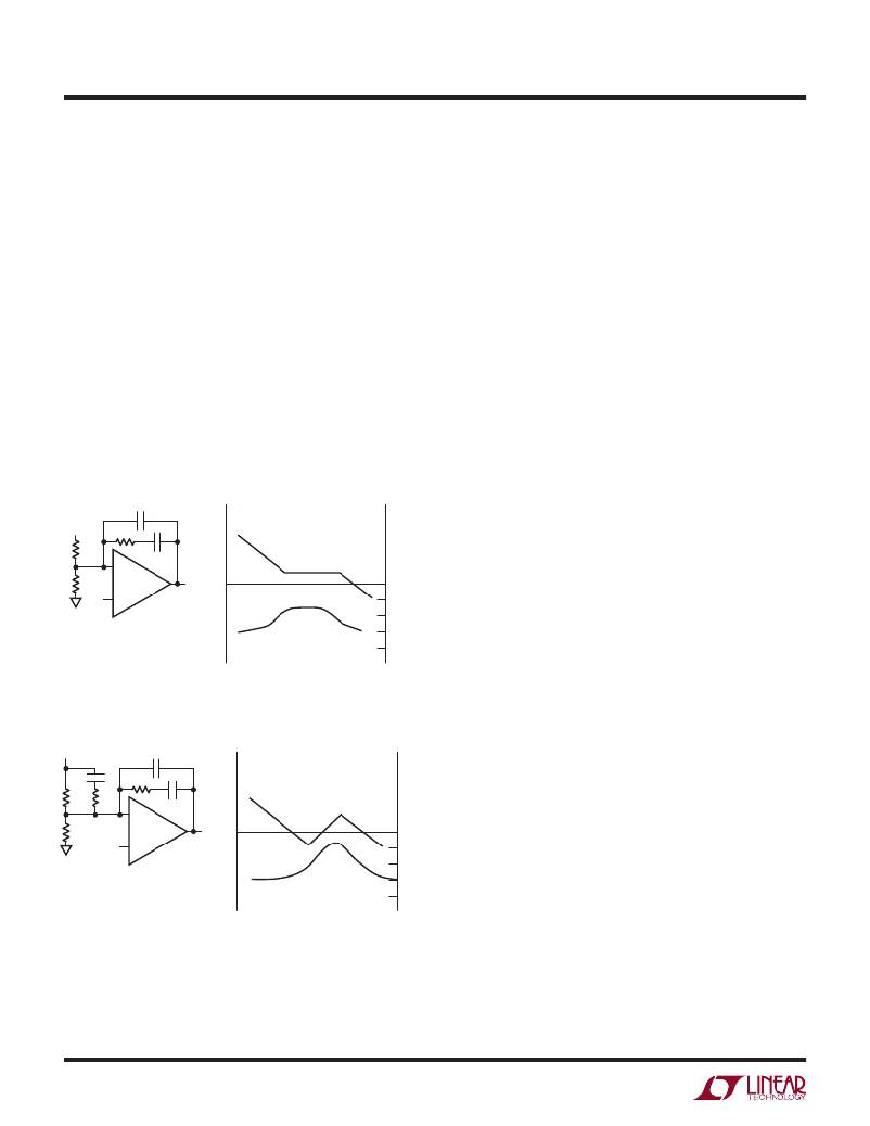
�The� two� types� of� compensation� networks,� “Type� 2”� and�
�“Type� 3”� are� shown� in� Figures� 11� and� 12.� When� compo-�
�nent� values� are� chosen� properly,� these� networks� provide�
�a� “phase� bump”� at� the� crossover� frequency.� Type� 2� uses�
�a� single� pole-zero� pair� to� provide� up� to� about� 60°� of� phase�
�boost� while� Type� 3� uses� two� poles� and� two� zeros� to� provide�
�up� to� 150°� of� phase� boost.�
�C2�
�C1�
�–6dB/OCT�
�GAIN�
�–6dB/OCT�
�R� FB2� OUT� 0� FREQ�
�V� REF� +� –90�
�–180�
�PHASE�
�–270�
�–360�
�38105� F11�
�Figure� 11.� Type� 2� Schematic� and� Transfer� Function�
�IN� C2�
�C1�
�R� FB1� R3� –6dB/OCT�
�FB�
�GAIN� +6dB/OCT� –6dB/OCT�
�R� FB2� OUT� 0� FREQ�
�V� REF� +� –90�
�PHASE� –180�
�–270�
�–360�
�38105� F12�
�Figure� 12.� Type� 3� Schematic� and� Transfer� Function�
�Feedback� Component� Selection�
�Selecting� the� R� and� C� values� for� a� typical� Type� 2� or� Type� 3�
�loop� is� a� nontrivial� task.� The� applications� shown� in� this�
�data� sheet� show� typical� values,� optimized� for� the� power�
�components� shown.� They� should� give� acceptable� perfor-�
�mance� with� similar� power� components,� but� can� be� way� off� if�
�even� one� major� power� component� is� changed� significantly.�
�Applications� that� require� optimized� transient� response� will�
�require� recalculation� of� the� compensation� values� specifically�
�for� the� circuit� in� question.� The� underlying� mathematics� are�
�complex,� but� the� component� values� can� be� calculated� in�
�a� straightforward� manner� if� we� know� the� gain� and� phase�
�of� the� modulator� at� the� crossover� frequency.�
�Modulator� gain� and� phase� can� be� obtained� in� one� of�
�three� ways:� measured� directly� from� a� breadboard,� or� if�
�the� appropriate� parasitic� values� are� known,� simulated� or�
�generated� from� the� modulator� transfer� function.� Mea-�
�surement� will� give� more� accurate� results,� but� simulation�
�or� transfer� function� can� often� get� close� enough� to� give�
�a� working� system.� To� measure� the� modulator� gain� and�
�phase� directly,� wire� up� a� breadboard� with� an� LTC3810-5�
�and� the� actual� MOSFETs,� inductor� and� input� and� output�
�capacitors� that� the� final� design� will� use.� This� breadboard�
�should� use� appropriate� construction� techniques� for� high�
�speed� analog� circuitry:� bypass� capacitors� located� close�
�to� the� LTC3810-5,� no� long� wires� connecting� components,�
�appropriately� sized� ground� returns,� etc.� Wire� the� feedback�
�amplifier� with� a� 0.1μF� feedback� capacitor� from� I� TH� to� FB�
�and� a� 10k� to� 100k� resistor� from� V� OUT� to� FB.� Choose� the�
�bias� resistor� (R� FB2� )� as� required� to� set� the� desired� output�
�voltage.� Disconnect� R� FB2� from� ground� and� connect� it� to�
�a� signal� generator� or� to� the� source� output� of� a� network�
�analyzer� to� inject� a� test� signal� into� the� loop.� Measure� the�
�gain� and� phase� from� the� I� TH� pin� to� the� output� node� at� the�
�positive� terminal� of� the� output� capacitor.� Make� sure� the�
�analyzer’s� input� is� AC� coupled� so� that� the� DC� voltages�
�present� at� both� the� I� TH� and� V� OUT� nodes� don’t� corrupt� the�
�measurements� or� damage� the� analyzer.�
�If� breadboard� measurement� is� not� practical,� a� SPICE�
�simulation� can� be� used� to� generate� approximate� gain/�
�phase� curves.� Plug� the� expected� capacitor,� inductor� and�
�MOSFET� values� into� the� following� SPICE� deck� and� gener-�
�ate� an� AC� plot� of� V� OUT� /V� ITH� with� gain� in� dB� and� phase� in�
�38105fd�
�24�
�相关PDF资料 |
PDF描述 |
|---|---|
| LTC3834EUFD#PBF | IC REG CTRLR BUCK PWM CM 20-QFN |
| RLB9012-152KL | INDUCTOR HI CURRNT RADIAL 1500UH |
| RBA32DCBD | CONN EDGECARD 64POS R/A .125 SLD |
| LTC1929CG-PG#PBF | IC REG CTRLR BUCK PWM CM 28-SSOP |
| RBA32DCBH | CONN EDGECARD 64POS R/A .125 SLD |
相关代理商/技术参数 |
参数描述 |
|---|---|
| LTC3810IG | 制造商:Linear Technology 功能描述: |
| LTC3810IG#PBF | 功能描述:IC REG CTRLR BUCK PWM CM 28-SSOP RoHS:是 类别:集成电路 (IC) >> PMIC - 稳压器 - DC DC 切换控制器 系列:- 标准包装:2,500 系列:- PWM 型:电流模式 输出数:1 频率 - 最大:500kHz 占空比:96% 电源电压:4 V ~ 36 V 降压:无 升压:是 回扫:无 反相:无 倍增器:无 除法器:无 Cuk:无 隔离:无 工作温度:-40°C ~ 125°C 封装/外壳:24-WQFN 裸露焊盘 包装:带卷 (TR) |
| LTC3810IG#TRPBF | 功能描述:IC REG CTRLR BUCK PWM CM 28-SSOP RoHS:是 类别:集成电路 (IC) >> PMIC - 稳压器 - DC DC 切换控制器 系列:- 标准包装:2,500 系列:- PWM 型:电流模式 输出数:1 频率 - 最大:500kHz 占空比:96% 电源电压:4 V ~ 36 V 降压:无 升压:是 回扫:无 反相:无 倍增器:无 除法器:无 Cuk:无 隔离:无 工作温度:-40°C ~ 125°C 封装/外壳:24-WQFN 裸露焊盘 包装:带卷 (TR) |
| LTC3810IUH-5#PBF | 功能描述:IC REG CTRLR BUCK PWM CM 32-QFN RoHS:是 类别:集成电路 (IC) >> PMIC - 稳压器 - DC DC 切换控制器 系列:- 标准包装:2,500 系列:- PWM 型:电流模式 输出数:1 频率 - 最大:500kHz 占空比:96% 电源电压:4 V ~ 36 V 降压:无 升压:是 回扫:无 反相:无 倍增器:无 除法器:无 Cuk:无 隔离:无 工作温度:-40°C ~ 125°C 封装/外壳:24-WQFN 裸露焊盘 包装:带卷 (TR) |
| LTC3810IUH-5#TRPBF | 功能描述:IC REG CTRLR BUCK PWM CM 32-QFN RoHS:是 类别:集成电路 (IC) >> PMIC - 稳压器 - DC DC 切换控制器 系列:- 标准包装:2,500 系列:- PWM 型:电流模式 输出数:1 频率 - 最大:500kHz 占空比:96% 电源电压:4 V ~ 36 V 降压:无 升压:是 回扫:无 反相:无 倍增器:无 除法器:无 Cuk:无 隔离:无 工作温度:-40°C ~ 125°C 封装/外壳:24-WQFN 裸露焊盘 包装:带卷 (TR) |
发布紧急采购,3分钟左右您将得到回复。