- 您现在的位置:买卖IC网 > PDF目录15310 > LTC3832-1ES8#TR (Linear Technology)IC REG CTRLR BUCK PWM VM 8-SOIC PDF资料下载
参数资料
| 型号: | LTC3832-1ES8#TR |
| 厂商: | Linear Technology |
| 文件页数: | 13/24页 |
| 文件大小: | 0K |
| 描述: | IC REG CTRLR BUCK PWM VM 8-SOIC |
| 标准包装: | 2,500 |
| PWM 型: | 电压模式 |
| 输出数: | 1 |
| 频率 - 最大: | 360kHz |
| 占空比: | 95% |
| 电源电压: | 3 V ~ 8 V |
| 降压: | 是 |
| 升压: | 无 |
| 回扫: | 无 |
| 反相: | 无 |
| 倍增器: | 无 |
| 除法器: | 无 |
| Cuk: | 无 |
| 隔离: | 无 |
| 工作温度: | -40°C ~ 85°C |
| 封装/外壳: | 8-SOIC(0.154",3.90mm 宽) |
| 包装: | 带卷 (TR) |
�� �
�
�LTC3832/LTC3832-1�
�APPLICATIO� S� I� FOR� ATIO�
�Diagram).� This� increases� the� G2� on-time� and� allows� the�
�charge� pump� capacitors� to� be� refreshed.�
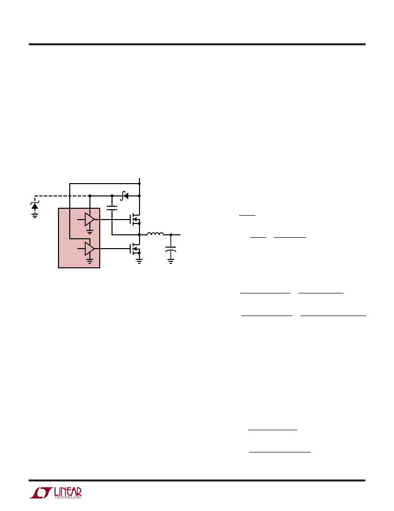
�For� applications� using� an� external� supply� to� PV� CC1� ,� this�
�supply� must� also� be� higher� than� V� CC� by� at� least� 2.5V� to�
�ensure� normal� operation.�
�For� applications� with� a� 5V� or� higher� V� IN� supply,� PV� CC2� can�
�be� tied� to� V� IN� if� a� logic� level� MOSFET� is� used.� PV� CC1� can� be�
�supplied� using� a� doubling� charge� pump� as� shown� in�
�Figure� 9.� This� circuit� provides� 2V� IN� –� V� F� to� PV� CC1� while� Q1�
�is� ON.�
�V� IN�
�enhance� standard� power� MOSFETs.� Under� this� condition,�
�the� effective� MOSFET� R� DS(ON)� may� be� quite� high,� raising�
�the� dissipation� in� the� FETs� and� reducing� efficiency.� Logic�
�level� FETs� are� the� recommended� choice� for� 5V� or� lower�
�voltage� systems.� Logic� level� FETs� can� be� fully� enhanced�
�with� a� doubler/tripling� charge� pump� and� will� operate� at�
�maximum� efficiency.�
�After� the� MOSFET� threshold� voltage� is� selected,� choose� the�
�R� DS(ON)� based� on� the� input� voltage,� the� output� voltage,�
�allowable� power� dissipation� and� maximum� output� current.�
�In� a� typical� LTC3832� circuit,� operating� in� continuous� mode,�
�the� average� inductor� current� is� equal� to� the� output� load�
�DC� (� Q� 1� )� =�
�OPTIONAL�
�USE� FOR� V� IN� ≥� 7V�
�D� Z�
�12V�
�1N5242�
�PV� CC2�
�PV� CC1�
�G1�
�MBR0530T1�
�0.1� μ� F�
�Q1�
�current.� This� current� flows� through� either� Q1� or� Q2� with� the�
�power� dissipation� split� up� according� to� the� duty� cycle:�
�V� OUT�
�V� IN�
�DC� (� Q� 2� )� =� 1� –� OUT� =� IN� OUT�
�G2�
�Q2�
�L� O�
�+�
�V� OUT�
�C� OUT�
�V� V� –� V�
�V� IN� V� IN�
�LTC3832�
�3832� F09�
�The� R� DS(ON)� required� for� a� given� conduction� loss� can� now�
�be� calculated� by� rearranging� the� relation� P� =� I� 2� R.�
�Figure� 9.� Doubling� Charge� Pump�
�Power� MOSFETs�
�R� DS� (� ON� )� Q� 1� =�
�P� MAX� (� Q� 1� )�
�DC� (� Q� 1� )� ?� (� I� LOAD�
�)� 2�
�=�
�V� IN� ?� P� MAX� (� Q� 1� )�
�V� OUT� ?� (� I� LOAD� )� 2�
�Two� N-channel� power� MOSFETs� are� required� for� most�
�LTC3832� circuits.� These� should� be� selected� based�
�primarily� on� threshold� voltage� and� on-resistance� consid-�
�R� DS� (� ON� )� Q� 2� =�
�P� MAX� (� Q� 2� )�
�DC� (� Q� 2� )� ?� (� I� LOAD� )� 2�
�=�
�V� IN� ?� P� MAX� (� Q� 2� )�
�(� V� IN� –� V� OUT� )� ?� (� I� LOAD� )� 2�
�R� DS� (� ON� )� Q� 1� =�
�=� 0� .� 011� ?�
�R� DS� (� ON� )� Q� 2� =� =� 0� .� 034� ?�
�erations. Thermal dissipation is often a secondary con-�
�cern� in� high� efficiency� designs.� The� required� MOSFET�
�threshold� should� be� determined� based� on� the� available�
�power� supply� voltages� and/or� the� complexity� of� the� gate�
�drive� charge� pump� scheme.� In� 3.3V� input� designs� where�
�an� auxiliary� 12V� supply� is� available� to� power� PV� CC1� and�
�PV� CC2� ,� standard� MOSFETs� with� R� DS(ON)� specified� at� V� GS�
�=� 5V� or� 6V� can� be� used� with� good� results.� The� current�
�drawn� from� this� supply� varies� with� the� MOSFETs� used�
�and� the� LTC3832’s� operating� frequency,� but� is� generally�
�less� than� 50mA.�
�LTC3832� applications� that� use� 5V� or� lower� V� IN� voltage� and�
�a� doubling/tripling� charge� pump� to� generate� PV� CC1� and�
�PV� CC2� ,� do� not� provide� enough� gate� drive� voltage� to� fully�
�P� MAX� should� be� calculated� based� primarily� on� required�
�efficiency� or� allowable� thermal� dissipation.� A� typical� high�
�efficiency� circuit� designed� for� 3.3V� input� and� 2.5V� at� 10A�
�output� might� allow� no� more� than� 3%� efficiency� loss� at� full�
�load� for� each� MOSFET.� Assuming� roughly� 90%� efficiency�
�at� this� current� level,� this� gives� a� P� MAX� value� of:�
�(2.5V)(10A/0.9)(0.03)� =� 0.83W� per� FET�
�and� a� required� R� DS(ON)� of:�
�(� 3� .� 3� V� )� ?� (� 0� .� 83� W� )�
�(� 2� .� 5� V� )(� 10� A� )� 2�
�(� 3� .� 3� V� )� ?� (� 0� .� 83� W� )�
�(� 3� .� 3� V� –� 2� .� 5� V� )(� 10� A� )� 2�
�sn3832� 3832fs�
�13�
�相关PDF资料 |
PDF描述 |
|---|---|
| VE-B2Z-EW-F1 | CONVERTER MOD DC/DC 2V 40W |
| LT1950EGN#TRPBF | IC REG CTRLR PWM CM 16-SSOP |
| LT1950EGN#TR | IC REG CTRLR PWM CM 16-SSOP |
| ASC05DRYI-S93 | CONN EDGECARD 10POS DIP .100 SLD |
| LTC3866EUF#TRPBF | IC REG CTRLR BUCK PWM CM 24-QFN |
相关代理商/技术参数 |
参数描述 |
|---|---|
| LTC3832EGN | 功能描述:IC REG CTRLR BUCK PWM VM 16-SSOP RoHS:否 类别:集成电路 (IC) >> PMIC - 稳压器 - DC DC 切换控制器 系列:- 标准包装:2,500 系列:- PWM 型:电流模式 输出数:1 频率 - 最大:500kHz 占空比:96% 电源电压:4 V ~ 36 V 降压:无 升压:是 回扫:无 反相:无 倍增器:无 除法器:无 Cuk:无 隔离:无 工作温度:-40°C ~ 125°C 封装/外壳:24-WQFN 裸露焊盘 包装:带卷 (TR) |
| LTC3832EGN#PBF | 功能描述:IC REG CTRLR BUCK PWM VM 16-SSOP RoHS:是 类别:集成电路 (IC) >> PMIC - 稳压器 - DC DC 切换控制器 系列:- 标准包装:2,500 系列:- PWM 型:电流模式 输出数:1 频率 - 最大:500kHz 占空比:96% 电源电压:4 V ~ 36 V 降压:无 升压:是 回扫:无 反相:无 倍增器:无 除法器:无 Cuk:无 隔离:无 工作温度:-40°C ~ 125°C 封装/外壳:24-WQFN 裸露焊盘 包装:带卷 (TR) |
| LTC3832EGN#TR | 功能描述:IC REG CTRLR BUCK PWM VM 16-SSOP RoHS:否 类别:集成电路 (IC) >> PMIC - 稳压器 - DC DC 切换控制器 系列:- 标准包装:2,500 系列:- PWM 型:电流模式 输出数:1 频率 - 最大:500kHz 占空比:96% 电源电压:4 V ~ 36 V 降压:无 升压:是 回扫:无 反相:无 倍增器:无 除法器:无 Cuk:无 隔离:无 工作温度:-40°C ~ 125°C 封装/外壳:24-WQFN 裸露焊盘 包装:带卷 (TR) |
| LTC3832EGN#TRPBF | 功能描述:IC REG CTRLR BUCK PWM VM 16-SSOP RoHS:是 类别:集成电路 (IC) >> PMIC - 稳压器 - DC DC 切换控制器 系列:- 标准包装:2,500 系列:- PWM 型:电流模式 输出数:1 频率 - 最大:500kHz 占空比:96% 电源电压:4 V ~ 36 V 降压:无 升压:是 回扫:无 反相:无 倍增器:无 除法器:无 Cuk:无 隔离:无 工作温度:-40°C ~ 125°C 封装/外壳:24-WQFN 裸露焊盘 包装:带卷 (TR) |
| LTC3832EG-T | 制造商:LINEAR TECHNOLOGY CORPORA 功能描述: 制造商:LINTEC 功能描述: |
发布紧急采购,3分钟左右您将得到回复。